Design and fabrication of 10-kV silicon–carbide p-channel IGBTs with hexagonal cells and step space modulated junction termination extension
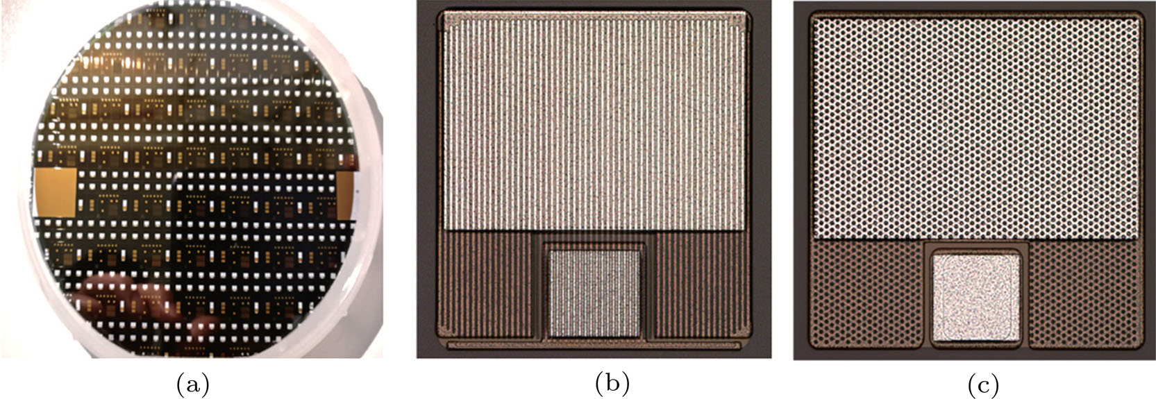
(color online) (a) Photograph of the fabricated IGBT wafer, (b) top-view photography of SiC IGBT with I-cell layout, (c) top-view photography of SiC IGBT with H-cell layout.