Research on SEE mitigation techniques using back junction and p+ buffer layer in domestic non-DTI SiGe HBTs by TCAD
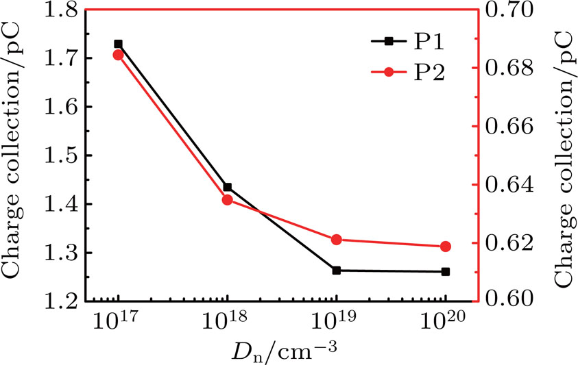
Plot of collector charge collection of back junction device versus Dn for P1 and P2.

Research on SEE mitigation techniques using back junction and p+ buffer layer in domestic non-DTI SiGe HBTs by TCAD |
|
Plot of collector charge collection of back junction device versus Dn for P1 and P2. |
 |