Research on SEE mitigation techniques using back junction and p+ buffer layer in domestic non-DTI SiGe HBTs by TCAD
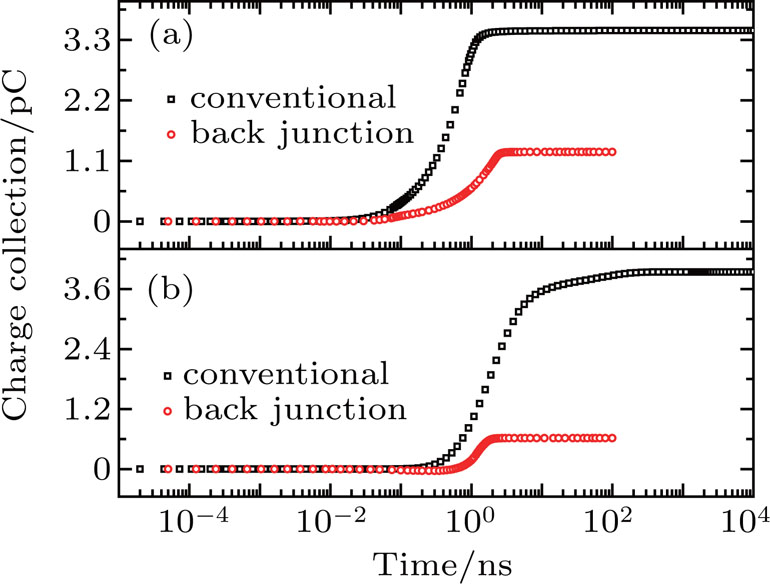
Plot of charge collection on collector in conventional and back junction HBT at (a) P1 and (b) P2.
Research on SEE mitigation techniques using back junction and p+ buffer layer in domestic non-DTI SiGe HBTs by TCAD |
|
Plot of charge collection on collector in conventional and back junction HBT at (a) P1 and (b) P2. |
| |