Epitaxial fabrication of two-dimensional TiTe2 monolayer on Au(111) substrate with Te as buffer layer
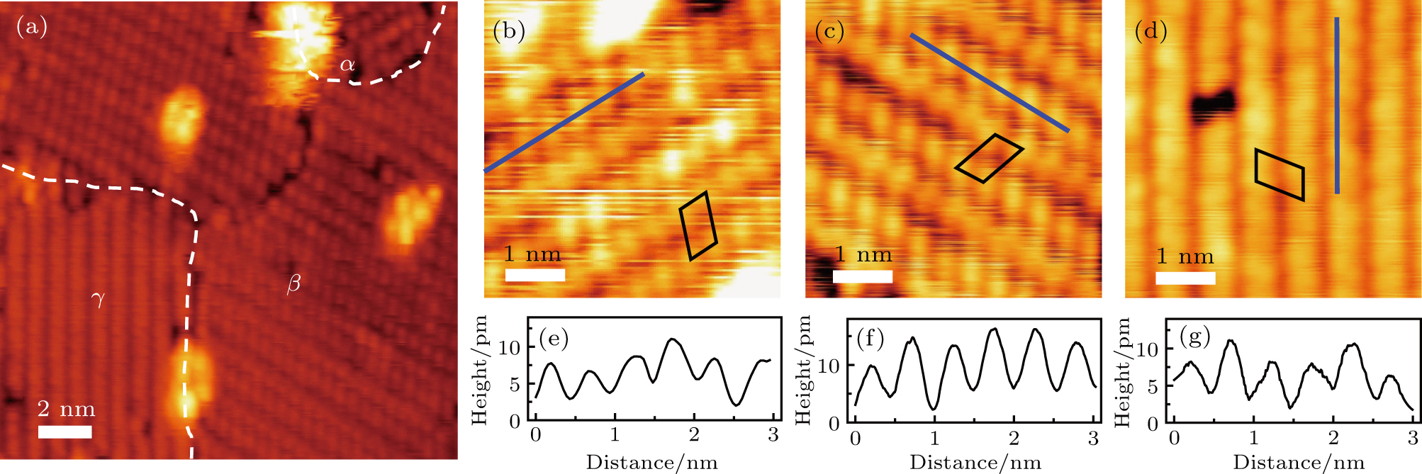
STM images of the 2D TiTe2 layer formed on the Au(111) surface. (a) STM image showing the three domains, marked as α, β, and γ. (b)–(d) Zoom-in STM images of the α, β, and γ domains in (a). (e)–(g) Line profiles of the purple lines in (b)–(d), respectively, which show periods of 5.0 Å, in agreement with
