† Corresponding author. E-mail:
We propose a novel structure for tunnel junction based on delta-doped AlGaAs/GaAs quantum wires. Higher spatial confinement of quantum wires alongside the increased effective doping concentration in the delta-doped regions extremely increase the peak tunneling current and enhance the performance of tunnel junction. The proposed structure can be used as tunnel junction in the multijunction solar cells under the highest possible thermodynamically limited solar concentration. The combination of the quantum wire with the delta-doped structure can be of benefit to the solar cells’ advantages including higher number of sub-bands and high degeneracy. Simulation results show a voltage drop of 40 mV due to the proposed tunnel junction used in a multijunction solar cell which presents an extremely low resistance to the achieved peak tunneling current.
Tunnel junctions (TJs) play a significant role in different optoelectronic devices. In multijunction solar cells, the tunnel junction allows photo-generated carriers to pass through the solar cell with minimum loss.[1] The multijunction solar cells used in higher solar-radiation concentrations have an essential requirement for tunnel junctions with high peak-to-valley current ratio,[2] which may be achieved by increasing the doping concentration of p- and n-type layers. However, it is hard to experimentally increase the doping concentration to a very high level.[3] For multijunction solar cells, the tunnel junction can provide a contact that exhibits high peak current, low resistive loss (i.e., voltage drop) and low optical loss. Both peak current and optical loss are related to the band gap in the junction region. As is well known, the tunneling process can be accelerated by creating an engineered energy level in order to gather the electrons. Utilizing the quantum confined structures is one of the methods for bandgap engineering aims. The investigation of energy-band diagrams emphasizes that the existence of internal sub-bands can greatly enhance the tunneling probability of carriers.[4] The internal sub-band region can be achieved by implementing the quantum well/wire structures through inserting a nano-scale low band-gap material between highly doped p- and n-type layers of the conventional tunnel junction.[5,6] It is obvious that the middle low band-gap layer makes a suitable region for the electrons established in the n-type region to be transmitted to the p-type region. So, the high carrier confinement in quantum-confined structure results in an improved tunnel device to be used in multijunction solar cells. However, in spite of recent improvement in quantum-structured tunnel junctions,[6,7] it seems that they cannot support the requirements for the future concentrated solar cells. Because the theoretical predictions based on thermodynamic limits and experimental achievements about highest possible solar concentration emphasize that the new multijunction solar cells require the improved tunnel junctions with the capability of passing the current density up to 
The high current density can be achieved with the extensive increase of doping concentration level. Most of the recent simulation-based researches focus on the highly-doped region in order to achieve a suitable peak tunneling current. However as previously explained, it is hard to implement very high p++ and n++ doping concentration. Therefore, we are trying to solve this problem by introducing a novel structure based on the reasonable doping concentrations. Delta-doping technique is a promising method which can be utilized to increase the effective doping concentration and consequently enhance the peak tunneling current of tunnel junction in comparison with those of the simple counterparts.[11,12]
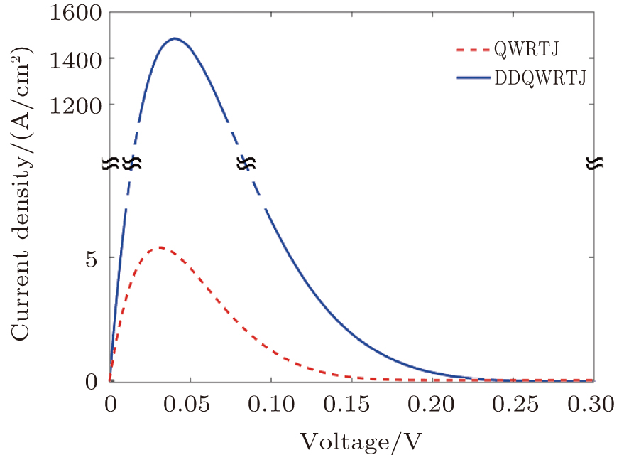
In this paper, a novel structure for tunnel junction is presented based on delta-doped quantum wires (DDQWRs) in order to extremely increase the tunneling probability. The proposed structure consists of five 6nm GaAs intrinsic quantum wires which are narrowly doped with p- and n-type materials in two 7.5 Å regions. Although the very high current density is not applicable according to limitations about the highest possible solar concentrations, the presented delta-doped quantum wire structure allows us to design the tunnel junctions with the capability of passing the tunneling current even higher than 1480 A/cm2 in the case. It should be mentioned that all of the experimental requirements have been considered in our simulations. The finite element method (FEM) is utilized to simulate the proposed tunnel junction. The simulation of transport of carriers through the structure can be accomplished by applying a set of differential equations, derived from Maxwellʼs equation, to grids.
The rest of this paper is organized as follows. In Section
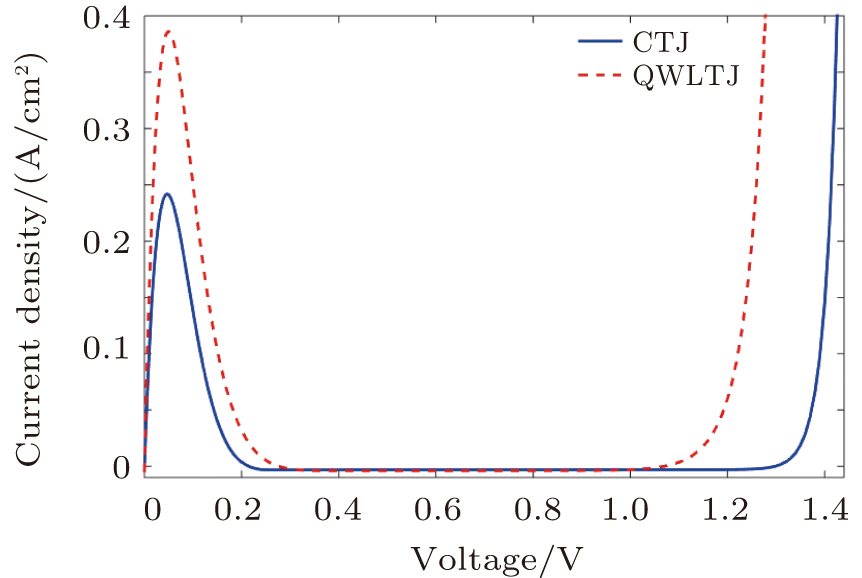
The low tunneling behavior of lightly-doped p–n junctions encouraged us to consider an Al0.3Ga0.7As p++–n++ tunnel structure with 5×1019 cm−3–3×1019 cm−3 doping concentration levels as a typical conventional tunnel junction (CTJ). This structure shows a peak tunneling current equal to 0.24 A/cm2, which is suitable for tunnel junctions of commonly used multijunction solar cells under lower multiple of solar concentration
As explained, the tunneling performance of conventional p++–n++ tunnel junction can be raised by introducing a quantum well structure between n- and p-type layers. However, the quantum well with doped barrier layers show higher influence than standard undoped quantum wells especially in the case of electron mobility.[13] According to this fact, our proposed quantum well tunnel junction (QWLTJ) is considered as a structure composed of an undoped GaAs layer sandwiched between two p++- and n++-AlGaAs barrier layers. Although the middle GaAs layer in QWLTJ with the lower energy band gap enhances the tunneling probability, the simulation results show that it does not increase the peak tunneling current considerably.
Using the low-dimensional structures provides a means to increase the peak current by reducing the effective band gap without increasing the absorption (loss) too much due to a reduced density of states.[6] Therefore, the quantum wire tunnel junction (QWRTJ) which can be experimentally produced by etching the undoped GaAs layer of quantum well structure can present a higher tunneling current. The width of and the gap between wires are considered to be 30nm which can be fabricated with new technologies.
Increasing the probability of tunneling, even increasing it up to a value much more than previous one, needs highly-degenerated structures. This is due to the fact that the conduction and valence band will be kept away from the Fermi level. To provide the mentioned high degeneracy, we make use of the delta-doping technique which is referred to as a doping distribution of semiconductors that is scaled down in one dimension to their ultimate spatial limits. It can be experimentally achieved by interrupting the crystal growth procedure and evaporation of dopants on the crystal surface.[14] The doping distribution of delta-doped structure which can be described with a two-dimensional δ-function, affects the local band gap. The conduction band energy of δ-function-like doping structure in the depth direction of z can be expressed as[11]

Equation (
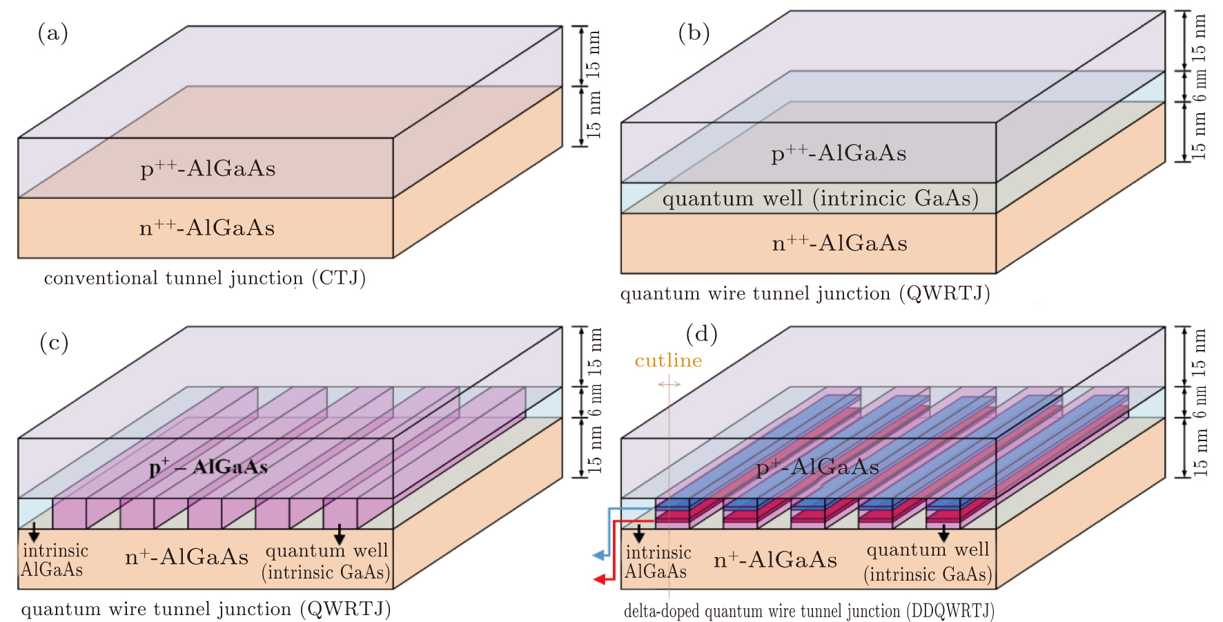 | Fig. 1. Schematic diagram of (a) conventional, (b) quantum well, (c) quantum wire, and (d) proposed delta-doped quantum wire tunnel junction. |
Figure
Firstly, we simulate an Al0.3Ga0.7As CTJ with a 5×1019 cm−3–3×1019 cm−3 doping concentration. However, to elevate the peak tunneling current, a quantum structure is utilized. Therefore, as can be seen in Fig.
As can be seen in Fig.
It is obvious that the quantum wire structure, shown in Fig.
As shown in Fig.
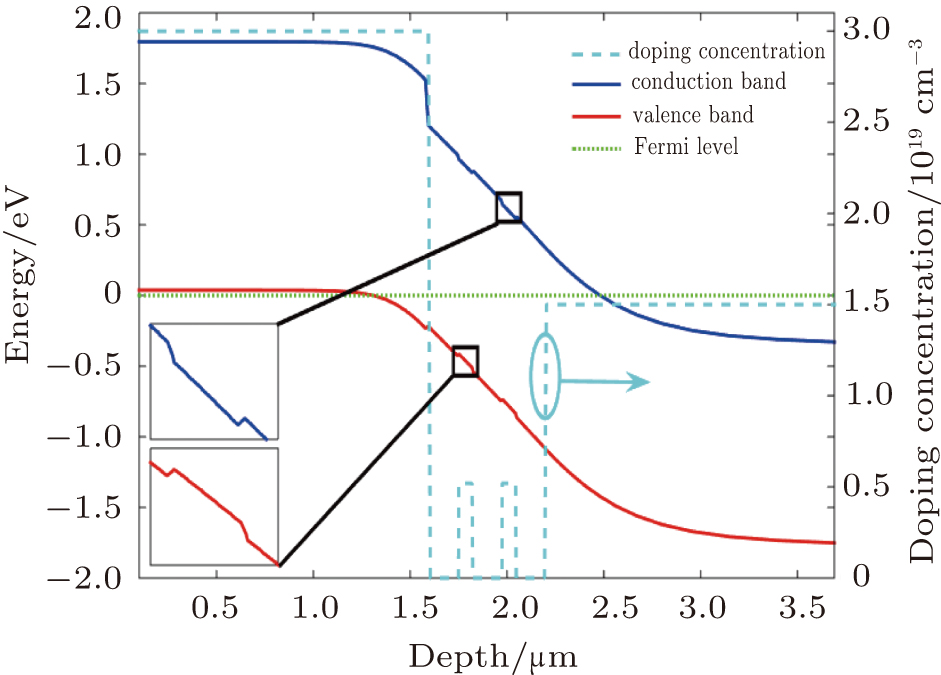
For a multijunction solar cell with typical short circuit current of almost 15 mA/cm2, the proposed structure with a peak tunneling current of 1480 A/cm2 can be utilized as a tunnel junction with a highest possible solar concentration. Also, as can be understood, utilizing the proposed tunnel junction in a multijunction solar cell results in a voltage drop of 40mV which is drastically low. So, due to the high peak current, the resistance of tunneling region extremely decreases. It is obvious that the internal sub-band of quantum wire structure increases the number of energy levels that can be occupied by the electrons. However, the extraordinary difference between a structure with delta-doping and a structure without delta-doping is because of the increase of tunneling probability due to local band gap displacement. The energy band diagram for a cutline shown in Fig.
As shown in Fig.
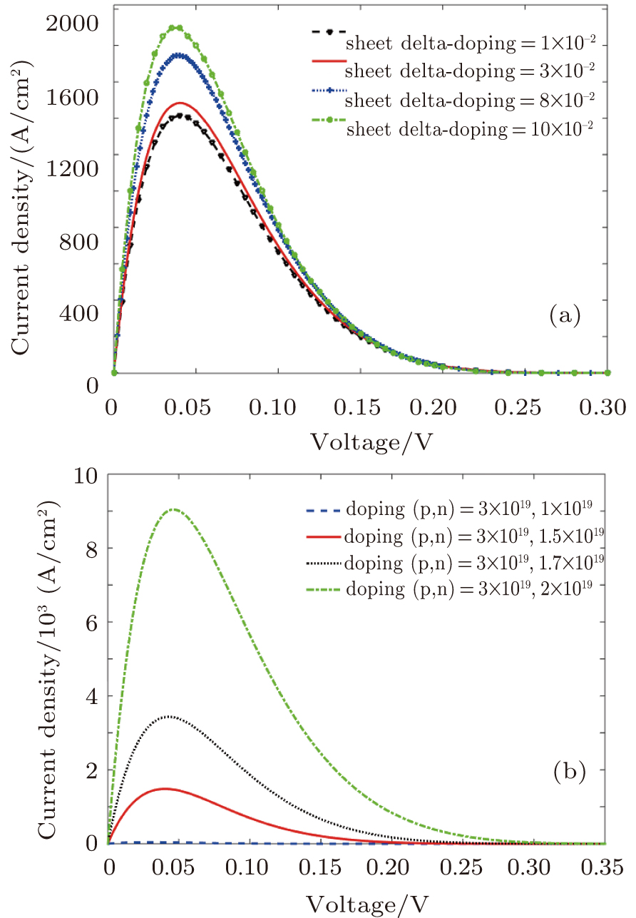
Simulation results show that the proposed structure presents the higher performance than the other counterparts even when the doping concentration of upper and lower AlGaAs layer are both reduced. Figure
As can be seen in Fig.
As previously mentioned, the proposed structure can be experimentally produced with 30-nm technology including deposition, photolithography and isotropic etching. It is worth noting that the performance of proposed device may be affected due to fabrication tolerance. In the case of our structure, there are two important parameters which can degrade the tunneling probability, i.e., the variations of doping of delta-doped regions and width of quantum wires. The effect of the mentioned parameters on the peak tunneling current density of structure is shown in Fig.
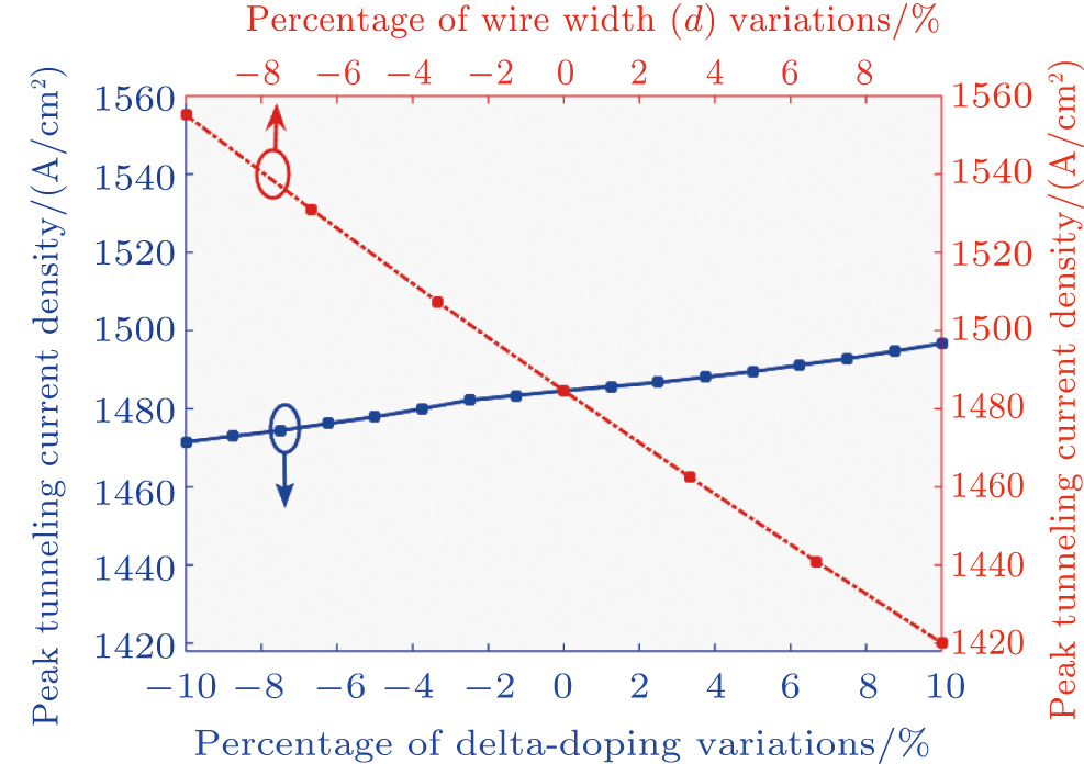 | Fig. 6. Peak tunneling current density versus relative variations of delta-doping level (blue) and width of quantum wire (red). |
The fabrication tolerance of the mentioned parameters is considered to be ± 10%. As can be seen in Fig.
Finally, it can be understood that the two-dimensional sheet doping concentrations can be more reduced with employing a higher number of delta-doped regions in order to achieve the same tunneling current.
A novel delta-doped AlGaAs/GaAs quantum wire tunnel junction is proposed. The combination of quantum wire structure with delta-doped structure allows us to simultaneously have their corresponding advantages including higher quantum confinement and high degeneracy. The comparison of I–V characteristics between conventional and quantum well, and the comparison between quantum wire tunnel junction and delta-doped quantum wire tunnel junction show a considerable enhancement for the later ones (i.e., for quantum well and delta-doped quantum wire tunnel junction). The proposed tunnel junction with a peak tunneling current of 1480 A/cm2 can be utilized for the highest possible solar concentration.
| [1] | |
| [2] | |
| [3] | |
| [4] | |
| [5] | |
| [6] | |
| [7] | |
| [8] | |
| [9] | |
| [10] | |
| [11] | |
| [12] | |
| [13] | |
| [14] |


