Room-temperature infrared photodetectors with hybrid structure based on two-dimensional materials
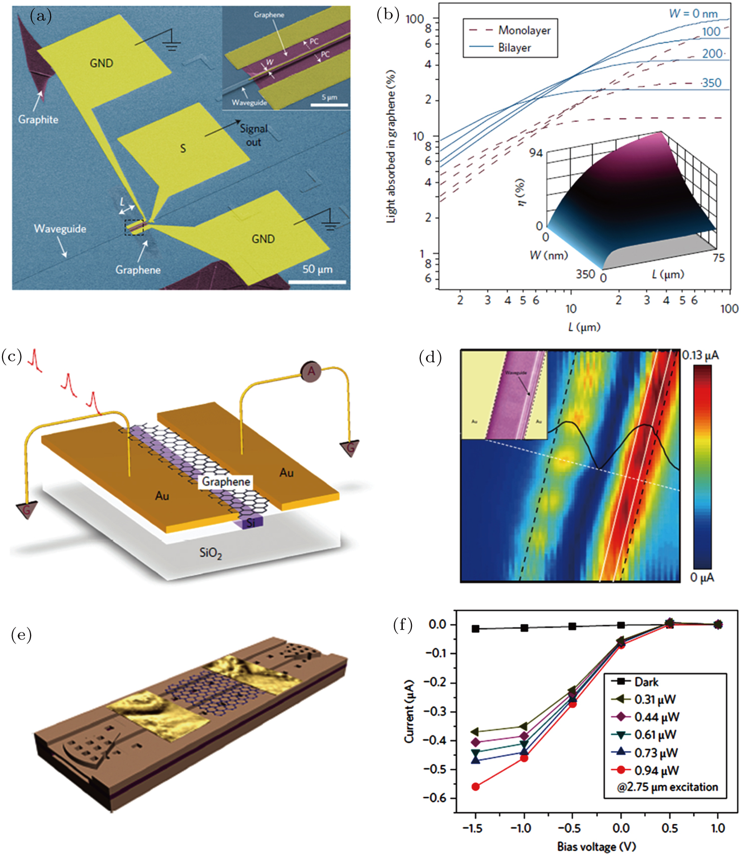
(a) SEM image of a waveguide-integrated graphene photodetector using a GND-S-GND configuration (false colour). Inset: an enlarged view of the inside of the black dashed line. (b) The absorption of graphene as a function of graphene length L at different widths W. Solid line: bilayer graphene. Dashed line: monolayer graphene. (c) Schematic of the chip-integrated graphene photodetector. (d) The spatially resolved photocurrent image of the waveguide-integrated graphene photodetector at zero bias. The black solid line shows the relative potential distribution across the graphene channel along the white dashed line. Inset: corresponding SEM image. (e) Schematic of a graphene/silicon heterostructure waveguide photodetector. (f) Photocurrent as a function of applied bias voltage with 
