|
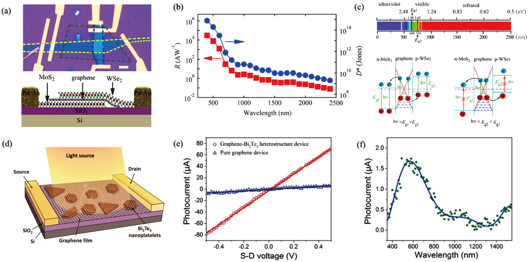
(a) Top: optical image of the photodetector based on a MoS2–graphene–WSe2 heterostructure. Bottom: schematic diagram of the device. scale bar,
10
μ
m
 . (b) Responsivity and specific detectivity of the photodetector for wavelengths ranging from 400 nm to 2400 nm with an interval of 100 nm. (c) Top: spectra from ultraviolet to infrared. The bandgap of MoS2 (Eg1) and WSe2 (Eg2) and the corresponding wavelengths are plotted on the graph, respectively. Bottom left: for
h
ν
>
E
g
1
>
E
g
2
. (b) Responsivity and specific detectivity of the photodetector for wavelengths ranging from 400 nm to 2400 nm with an interval of 100 nm. (c) Top: spectra from ultraviolet to infrared. The bandgap of MoS2 (Eg1) and WSe2 (Eg2) and the corresponding wavelengths are plotted on the graph, respectively. Bottom left: for
h
ν
>
E
g
1
>
E
g
2
 , MoS2, graphene, and WSe2 all can generate photogenerated electron–hole pairs. Bottom right: for
h
ν
<
E
g
1
<
E
g
2
, MoS2, graphene, and WSe2 all can generate photogenerated electron–hole pairs. Bottom right: for
h
ν
<
E
g
1
<
E
g
2
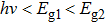 , only graphene can generate photogenerated electron–hole pairs. (d) The schematic diagram of the device based on graphene–Bi2Te3 heterostructure. (e) The dependence of photocurrent of devices based on pure graphene and graphene–Bi2Te3 heterostructure on source-drain voltage VSD. VG=0 V. (f) Dependence of photocurrent on wavelengths ranging from 400 nm to 1550 nm. Panels (a)–(c) are reproduced from Ref. [79] with permission from the American Chemical Society. Panels (d)–(f) are reproduced from Ref. [82] with permission from the American Chemical Society.
|