Room-temperature infrared photodetectors with hybrid structure based on two-dimensional materials
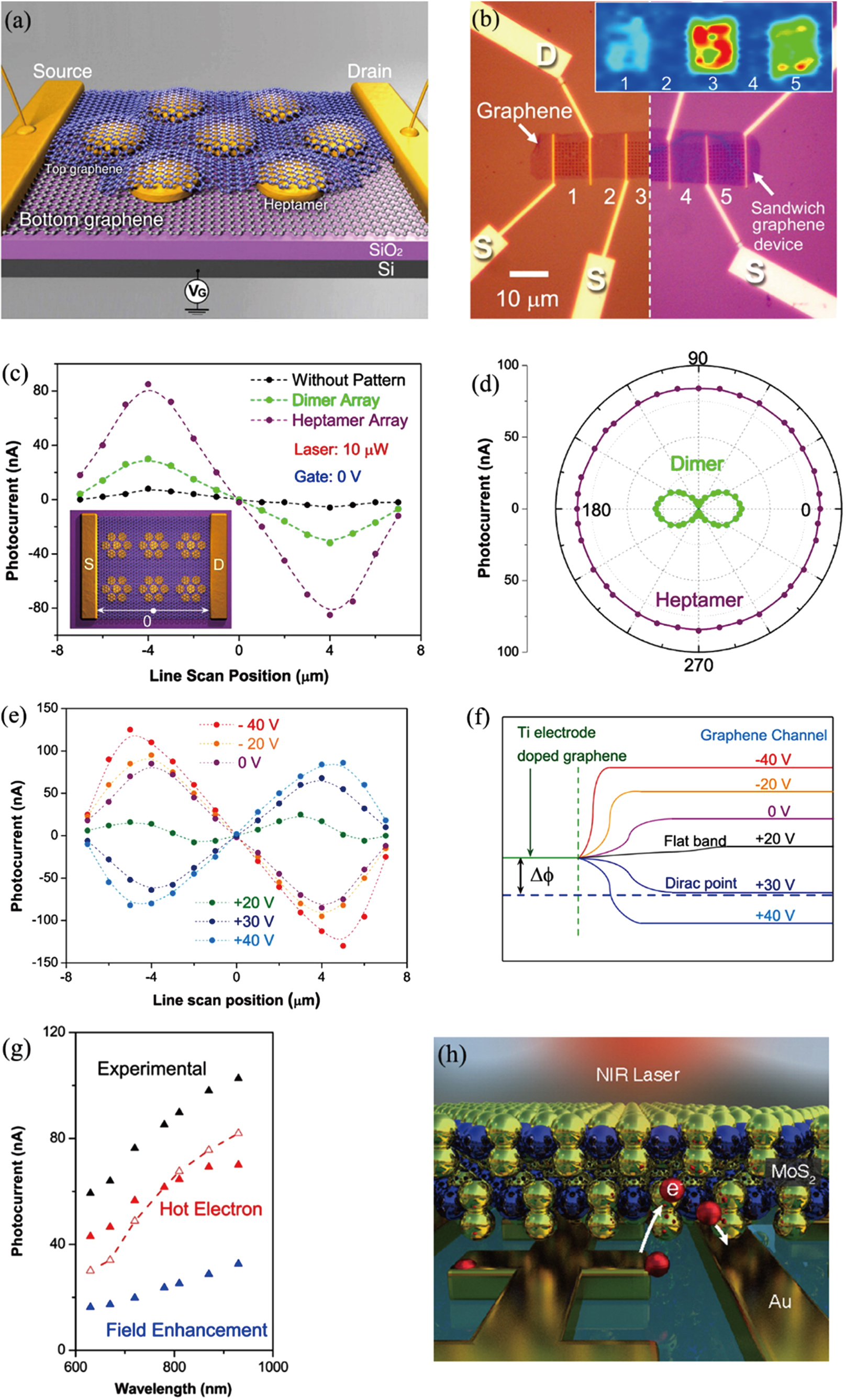
(a) The schematic of graphene–antenna sandwich photodetector. (b) The optical image of device before (left) and after (right) transfer of top layer graphene. Inset: Raman mapping of the device under 785 nm laser illumination. (c) Photocurrents measured in the photodetector with dimer array and heptamer array and without pattern exhibit antisymmetric properties. The results show that the metal plasmonic antenna clusters can effectively enhance the photocurrent. The line scan position is shown by the white arrows in the inset. (d) The polarization-dependent properties of the photocurrent measured in dimer and heptamer devices. (e) Photocurrents measured at different gate voltages in a heptamer device. (f) Energy band diagram of devices with different gate voltages in a heptamer device. The purple dashed line indicates the Dirac point of graphene. (g) Photocurrent as a function of resonant wavelength. Black triangles: the measured photocurrent (IEXP(λ)). Blue triangles: the calculated DE photocurrent (IDE(λ)). Solid red triangles: the estimated HE photocurrent contribution EDE(λ)=IEXP(λ)–IDE(λ). Hollow red triangles: the calculated IHE(λ). (h) Schematic of hot electron-based bilayer MoS2 with near-infrared laser illumination. Panels (a)–(g) are reproduced from Ref. [
