Photodetectors based on two-dimensional materials and organic thin-film heterojunctions*

Project supported by National Science Funds for Creative Research Groups of China (Grant No. 61421002).

Han Jiayue1, Wang Jun1, 2, †
       

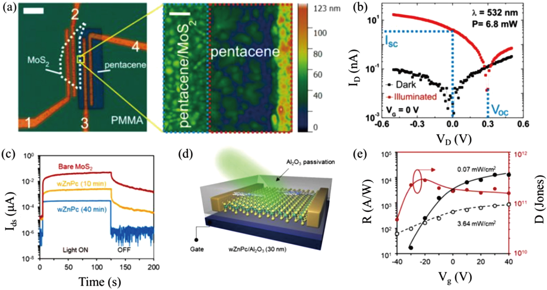
(a) Optical micrograph of a representative MoS2/pentacene p–n junction (left panel, scale bar is 10 μm). The AFM image of the MoS2/pentacene p–n junction area (right panel, scale bar is 500 nm).[104] (b) The current–voltage characteristics of p–n junctions without VG in the dark and under light illumination.[104] (c) The time-dependent photoresponse measurement of the MoS2 device and MoS2 with various ZnPc treatments.[107] (d) The diagram of MoS2/ZnPc with an Al2O3 passivation layer photodetector structure.[107] (e) Gate-modulated responsivity and detectivity of the MoS2/ZnPc photodetector with Al2O3 passivation at a power intensity of 0.07 and 3.64 mW/cm2.[107]