Li Xiang, Sun Jian-Dong, Huang Hong-Juan, Zhang Zhi-Peng, Jin Lin, Sun Yun-Fei, Popov V V, Qin Hua. The origin of distorted intensity pattern sensed by a lens and antenna coupled AlGaN/GaN-HEMT terahertz detector*
Project supported by the National Key Research and Development Program of China (Grant No. 2016YFF0100501), the National Natural Science Foundation of China (Grant Nos. 61771466, 61775231, and 61611530708), the Six Talent Peaks Project of Jiangsu Province, China (Grant No. XXRJ-079), the Youth Innovation Promotion Association of Chinese Academy of Sciences (Grant No. 2017372), the Russian Foundation for Basic Research (Grant No. 17-52-53063), and the Natural Science Foundation of Jiangsu Province, China (Grant No. BK20160400).
. Chinese Physics B, 2019, 28(11): 118502
Permissions
The origin of distorted intensity pattern sensed by a lens and antenna coupled AlGaN/GaN-HEMT terahertz detector*
Project supported by the National Key Research and Development Program of China (Grant No. 2016YFF0100501), the National Natural Science Foundation of China (Grant Nos. 61771466, 61775231, and 61611530708), the Six Talent Peaks Project of Jiangsu Province, China (Grant No. XXRJ-079), the Youth Innovation Promotion Association of Chinese Academy of Sciences (Grant No. 2017372), the Russian Foundation for Basic Research (Grant No. 17-52-53063), and the Natural Science Foundation of Jiangsu Province, China (Grant No. BK20160400).
Li Xiang1, 2, Sun Jian-Dong1, †, Huang Hong-Juan3, Zhang Zhi-Peng1, Jin Lin1, Sun Yun-Fei4, Popov V V5, Qin Hua1, ‡
Key Laboratory of Nanodevices and Applications, Suzhou Institute of Nano-tech and Nano-bionics, Chinese Academy of Sciences, Suzhou 215123, China
School of Nano Technology and Nano Bionics, University of Science and Technology of China, Hefei 230026, China
Nanofabrication Facility of the Suzhou Institute of Nano-tech and Nano-bionics, Chinese Academy of Sciences, Suzhou 215123, China
College of Electronic and Information Engineering, Suzhou University of Sciences and Technology, Suzhou 215009, China
Kotelnikov Institute of Radio Engineering and Electronics, Saratov Branch, Russian Academy of Sciences, Saratov 410019, Russia
Project supported by the National Key Research and Development Program of China (Grant No. 2016YFF0100501), the National Natural Science Foundation of China (Grant Nos. 61771466, 61775231, and 61611530708), the Six Talent Peaks Project of Jiangsu Province, China (Grant No. XXRJ-079), the Youth Innovation Promotion Association of Chinese Academy of Sciences (Grant No. 2017372), the Russian Foundation for Basic Research (Grant No. 17-52-53063), and the Natural Science Foundation of Jiangsu Province, China (Grant No. BK20160400).
Abstract
Antenna-coupled field-effect-transistors (FETs) offer high sensitivity for terahertz detection. Both the magnitude and the polarity of the response signal are sensitive to the localized terahertz field under the gate. The ability of accurate sensing the intensity pattern is required for terahertz imaging systems. Here, we report artefacts in the intensity pattern of a focused terahertz beam around 1 THz by scanning a silicon-lens and antenna coupled AlGaN/GaN high-electron-mobility-transistor (HEMT) detector. The origin of the image distortion is found to be connected with one of the antenna blocks by probing the localized photocurrents as a function of the beam location and the frequency. Although the exact distortion is found with our specific antenna design, we believe similar artefacts could be commonplace in antenna-coupled FET terahertz detectors when the beam spot becomes comparable with the antenna size. To eliminate such artefacts, new antenna designs are welcomed to achieve strong asymmetry in the terahertz field distribution under the gate while maintaining a more symmetric radiation pattern for the whole antenna.
Sensitive terahertz sensors are one of the key devices in terahertz application systems, for example, terahertz imagers and scanners.[1–8] Such systems usually require direct detection of the terahertz power,[9] while some other systems, for example, coherent sensing systems need detection of phase as well.[10–12] Terahertz detectors and array for imaging applications require a precise response to the spatially distributed terahertz power of the incoming terahertz wave. An antenna-coupled field-effect-transistor (FET) terahertz detector receives the incident terahertz wave by the integrated onchip antenna and generates a self-mixing current. Since it is the asymmetry that ensures the generation of an unidirectional self-mixing current,[13–16] an asymmetric antenna is required to make the self-mixing more effective. For this purpose, a few different types of antennas or couplers have been realized and examined in FET-based detectors.[17–23] Recently, Boppel et al. found that an FET detector coupled with symmetric antennas is able to detect the intensity gradient and hence allows for direct edge detection.[14] They further pointed out that the asymmetry in the antenna-coupled FETs has to be assured so that the devices can be used as pure power detectors and become insensitive to the intensity gradient. For sensing and imaging applications, silicon lenses are widely used to greatly improve the coupling efficiency and hence the sensitivity by focusing the terahertz wave onto the active regions of the detectors.[23–25] Unlike optoelectronic detectors for shorter wavelength radiation in which the dimension of the detector area is greater than the wavelength, the integration of FET detectors with silicon lenses may induces a beam spot size comparable to the antenna. The detector response becomes sensitive to the location of the focused beam relative to the antenna and gives rise to unpredicted changes not only in the magnitude but also in the photocurrent direction in some circumstances. Hence, careful design of the antenna and accurate alignment of the antenna to the silicon lens are needed to avoid unwanted artefacts in the terahertz imaging system. In this work, we report raster scanned images of a focused terahertz beam by using an antenna-coupled highelectron- mobility-transistor (HEMT) detector integrated on a silicon lens. An image distortion is found to be related with the frequency and the relative location between the focused beam and the antenna. Possible solutions to eliminate this type of artefacts are discussed.
2. Experimental setup
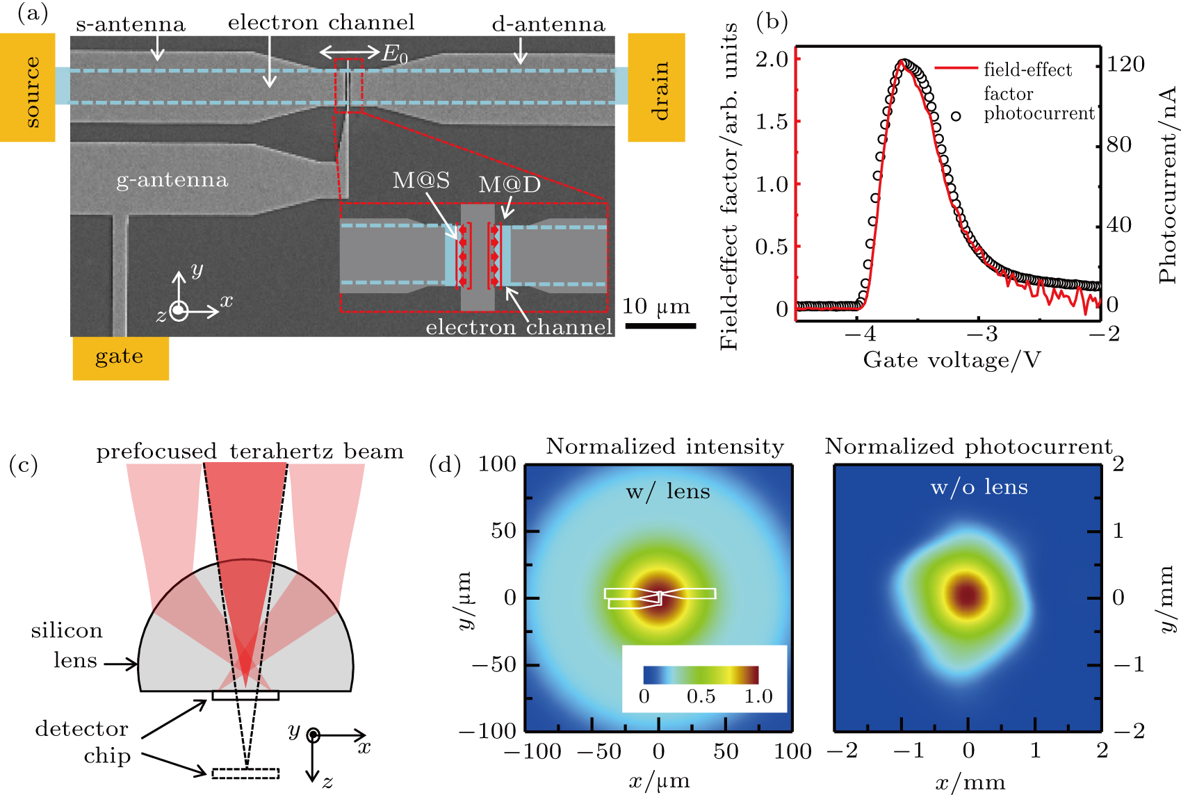
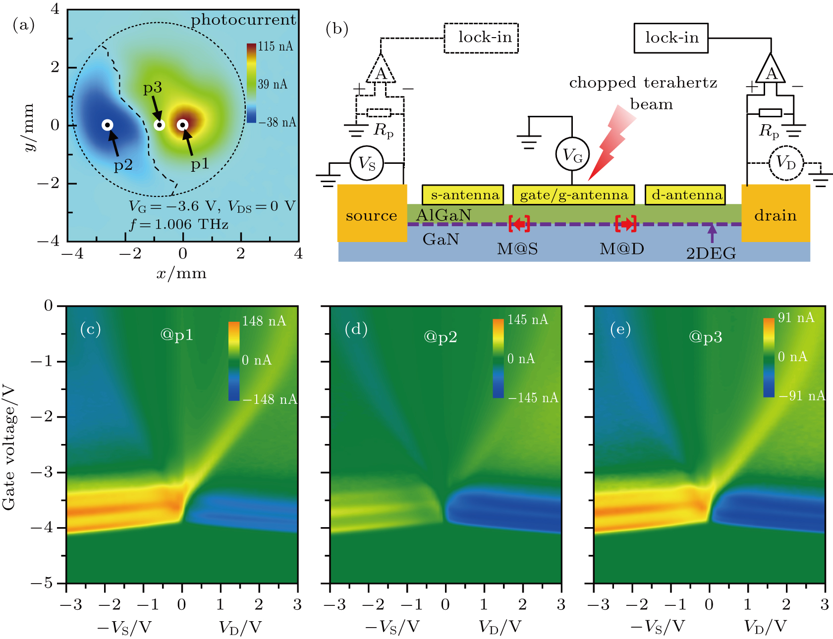
The terahertz detector is an antenna-coupled HEMT fabricated based on AlGaN/GaN heterostructure with a sapphire substrate. The fabrication process has been introduced in details in our previous reports.[15,26] As shown in Fig. 1(a), the key design is the asymmetric dipole antenna which includes three blocks each having a length of 45 μ m optimized for the terahertz wave at 0.9 THz. Along with d-antenna and s-antenna, g-antenna connected with the gate induces a strongly localized terahertz field near the edges of the gated electron channel marked by M@D and M@S. The field-effect gate has a length of L = 200 nm and a width of W = 4 μm.
Fig. 1. (a) Scanning-electron micrograph of antenna-coupled HEMT. (b) Measured field-effect factor and photocurrent at different gate voltages. (c) Schematic of the detector integrated on a silicon lens and the incident terahertz beam. (d) Simulated intensity pattern (left) focused by the silicon lens and measured intensity pattern (right) without silicon lens.
As reported earlier in Ref. [26], the terahertz detector consists of the terahertz antenna and the HEMT. The incident terahertz beam reaches the channel of the HEMT, after collected by the terahertz antenna, induces an electric field in the channel. There exist two terahertz field components (Ex and Ez) in the gated electron channel, one alone direction x, i.e., from source to drain, the other in z, i.e., perpendicular to the plane of the channel. The self-mixing current generated in M@S or M@D is proportional to the product of the two field components. Due to the phase change of π between field components Ez in areas M@S and M@D, a negative self-mixing current and a positive self-mixing current are generated in areas M@S and M@D, respectively, as schematically illustrated by the red arrows in brackets in Fig. 1(a). The sum of the local current along the gated electron channel gives the overall output short-circuit photocurrent. When no source–drain bias is applied, the output photocurrent is proportional to the so-called antenna factor , where and are the terahertz field enhancement factors. The instant terahertz field component Ex induced in the gated electron channel experiences a phase flip of π from the gated channel on the drain side to that on the source side, while field components Ez keeps in phase along the gated channel. Phase difference ϕ is defined to represent the instant difference between the polarities of the mixing terahertz field components, i.e., the product of Ex and Ez. E0 is the free space field strength of the incident wave. We assume that the light intensity of the incident terahertz beam distributes evenly on the surface of the device, and simulate the distribution of the induced electric field in the channel by FDTD solutions, and then calculate the antenna factor Λ in M@D and M@S. The ratio of the field strength between M@D and M@S is found to be about 2.7. Such asymmetric field distribution is essential for the device to create an unidirectional photocurrent. The overall and local photocurrents reflect the intensity of the terahertz field confined under the gate. Apart from the antenna factor, the field-effect factor Ξ = dn/dVG, which counts for the ability of tuning the electron density by the gate voltage and the terahertz field perpendicular to the channel plane, is the other important factor for detection. Considering the effect of the series resistance r of the ohmic contacts and the long mesa,[SunAPL1] the field-effect factor could be redefined as Ξ = dn/(d VG(1 + rG0)), where G0 is the conduct of the detector. The larger the antenna factor and the field-effect factor, the higher the photocurrent iT ∝ ΞΛ. As shown in Fig. 1(b), the induced photocurrent is coincident well with the field-effect factor, and maximized at −3.6 V.
Attempts to enhance the photocurrent include increase of the field-effect factor, increase of the terahertz field strength in one of the mixing areas, and increase of the degree of asymmetry in the field distribution. In our specific antenna design, since the strength of the mixing factor in M@S is about one third of that in M@D, there is a significant fraction of mixing current in M@D which is compensated by the opposite current in M@S.[15] When the terahertz beam is focused down to a diameter about 1 mm by using a three-inch-diameter offaxis parabolic (OAP) mirror, no negative photocurrent can be probed in such detector without silicon lens. However, a negative photocurrent can be extracted from such bare detectors even without silicon lens by applying a positive source–drain bias on the drain to deplete the electron channel and hence suppress the positive self-mixing current in M@D.[26] In this work, the terahertz beam before the silicon lens is prefocused by an OAP mirror and the detector is mounted in the center of a hyperspherical silicon lens with a diameter of 6 mm, as schematically shown in Fig. 1(c). Finite-element simulation indicates that a 1.006 THz terahertz beam focused by the silicon lens is about 72 μ m in full-width-at-half-magnitude (FWHM), as shown in Fig. 1(d), i.e., the beam spot is slightly smaller than the total antenna length (90 μ m). In comparison, the prefocused terahertz beam has a beam size of 1 mm in FWHM, as shown in the right pattern of Fig. 1(d), which is more than 13 times larger than that shown in Fig. 1(d). The application of the silicon lens and scan of the lens-integrated detector relative to the prefocused beam allow for shifting the focused beam spot on the detector chip, as schematically shown in Fig. 1(c).
3. Results and discussion
By applying a gate voltage of −3.6 V and a zero source–drain bias, the lens-integrated detector is used to scan the prefocused terahertz beam at 1.006 THz. The obtained image of the photocurrent is shown in Fig. 2(a). Unlike the Gaussian intensity image shown in Fig. 1(d), the intensity pattern can be clearly separated into two regions with opposite photocurrents: negative in the left part and positive in the right part. The area with positive photocurrent is larger than that with negative photocurrent. This unexpected pattern indicates that the self-mixing currents generated in M@S and M@D are altered by the beam shifted between the s-antenna and d-antenna. In between the positive and negative regions, there exists a zero-boundary along which the photocurrent is minimized. To identify the different situations, we define three positions marked by p1, p2, and p3, corresponding to the maximum positive photocurrent (+115 nA), the maximum negative photocurrent (−38 nA), and the intermediate photocurrent (+44.3 nA), respectively, as shown in Fig. 2(a). The distance between p1 and p2 is 2.6 mm, the zero-boundary is 1.4 mm to p1 and 1.2 mm to p2. Point p3 is 0.8 mm to p1 and 1.8 mm to p2. The ratio of the photocurrent between p1 and p2 is about 3.0 which is close to the ratio (≈ 2.7) of the simulated antenna factors in M@D and M@S. Although the exact location of the focused beam relative to the antenna cannot be obtained in the current setup, a rough estimation can be made based on the optical configuration: a positive photocurrent is generated when the beam is deflected to the d-antenna side and a negative photocurrent is induced when the beam is shifted to the s-antenna side.
Fig. 2. (a) Measured photocurrent pattern of a prefocused beam by raster scanning the detector with a silicon lens. (b) Schematic setup for extracting the local self-mixing current. The solid/dashed circuitry is for probing photcurrent in M@D/M@S, respectively. Local photocurrent probed at (c) p1, (d) p2, and (e) p3.
As shown in Fig. 2(b), a positive bias applied either on the drain or on the source depletes the corresponding part of the electron channel (M@D, M@S). This method allows for full extraction of the positive photocurrent in M@D and the negative photocurrent in M@S when the beam is deflected. The photocurrent as a function of the source–drain bias and the gate voltage mapped at p1, p2, and p3 is shown in Figs. 2(c)–2(e), respectively. In case p1, i.e., the beam spot is shifted towards d-antenna, the positive bias applied on the source allows to extract the positive photocurrent in M@D (+148 nA). Instead, when the positive bias is applied on the drain, the negative photocurrent in M@S is extracted. The negative current (−77.0 nA) in M@S is about 0.52 of the positive current. In case p2, i.e., the beam spot is shifted towards s-antenna, the positive bias applied on the drain reveals the negative photocurrent (−141.7 nA) in M@S. When the positive bias is applied on the drain, the positive photocurrent (+60.5 nA) in M@D is then extracted. In case p3, i.e., the beam spot is roughly in between the s-antenna and d-antenna, the positive current (+89 nA) and the negative photocurrent (−87 nA) tuned by the bias become rather equalized in magnitude. In cases of p1 and p2, the ratios of the photocurrent between M@D and M@S are 1.92 and 2.32, respectively, both are smaller than the ratio (3.0) when no bias is applied. This is reasonable since the beam spot is strongly shifted to d-antenna/s-antenna and the local self-mixing in M@D/M@S is mostly determined by the d-antenna/s-antenna. The inline configuration of g-antenna and d-antenna helps to enhance the field in M@D. On the contrary, even when the beam is shifted towards s-antenna, the local terahertz field in M@S is slightly suppressed by g-antenna which is in parallel with s-antenna. The above results indicate that self-mixing in M@S and M@D always exists even when the beam is strongly deflected to d-antenna and s-antenna, respectively.
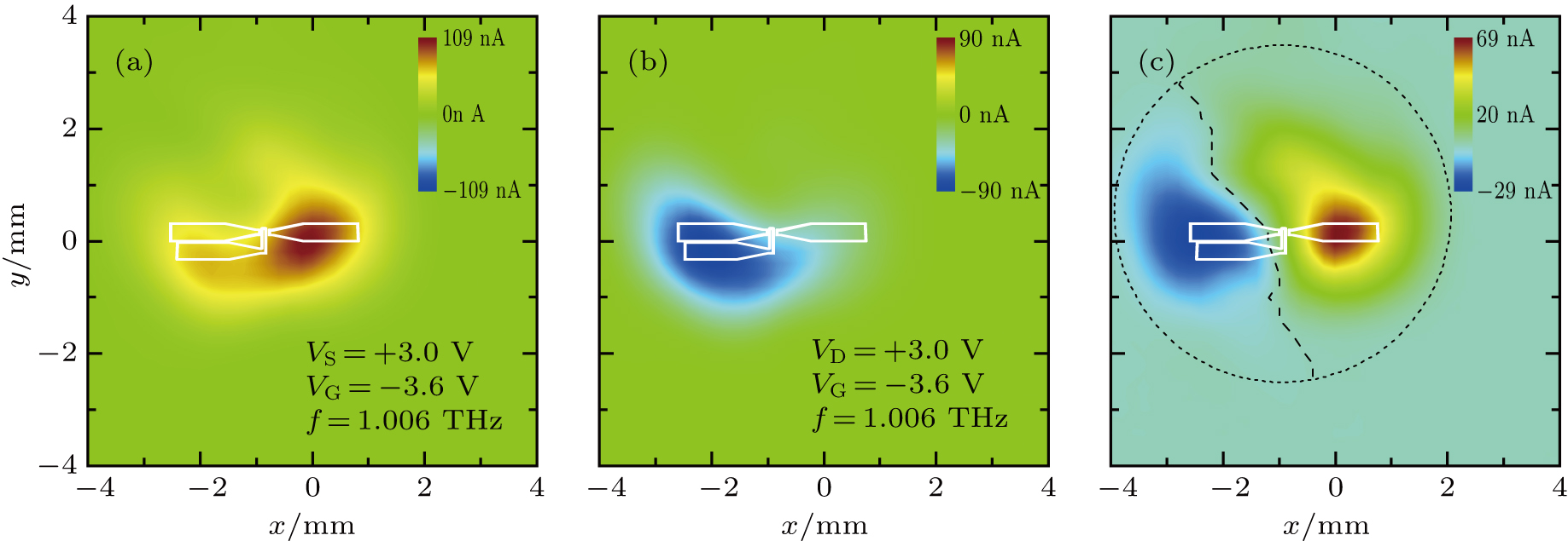
The local self-mixing in M@S and M@D can be effectively switched off by depleting the corresponding electron channel. We examine the images of the same focused beam by applying a +3.0 V bias to the source or the drain, as shown in Figs. 3(a) and 3(b), respectively. As expected, only positive photocurrent and only negative photocurrent are observed in Figs. 3(a) and 3(b), respectively. The raster-scanned intensity patterns are different since the geometric configurations between the beam and the effective antennas are different. A sum of the photocurrent shown in Figs. 3(a) and 3(b) is plotted in Fig. 3(c), which shows a very similar pattern to that in Fig. 2(a) obtained when no bias is applied. Both d-antenna and g-antenna contribute to the positive self-mixing current in M@D, while s-antenna and g-antenna contribute to the negative self-mixing current in M@S. The ratio of the maximum positive current (Fig. 3(a)) to the maximum negative current (Fig. 3(b)) is about 1.2 which indicates the self-mixing in M@D and M@S is mainly determined by d-antenna and s-antenna, respectively. The deviation of this ratio from 1.0 reflects that the difference between the inline configuration of d-antenna and g-antenna and the parallel configuration of s-antenna and g-antenna.
Fig. 3. Photocurrent patterns obtained by raster scanning the detector with silicon lens when a +3 V bias is applied (a) on the source or (b) on the drain. (c) Sum of the patterns shown in (a) and (b). The antenna is magnified and overlayed as a guide for the beam location relative to the antenna.
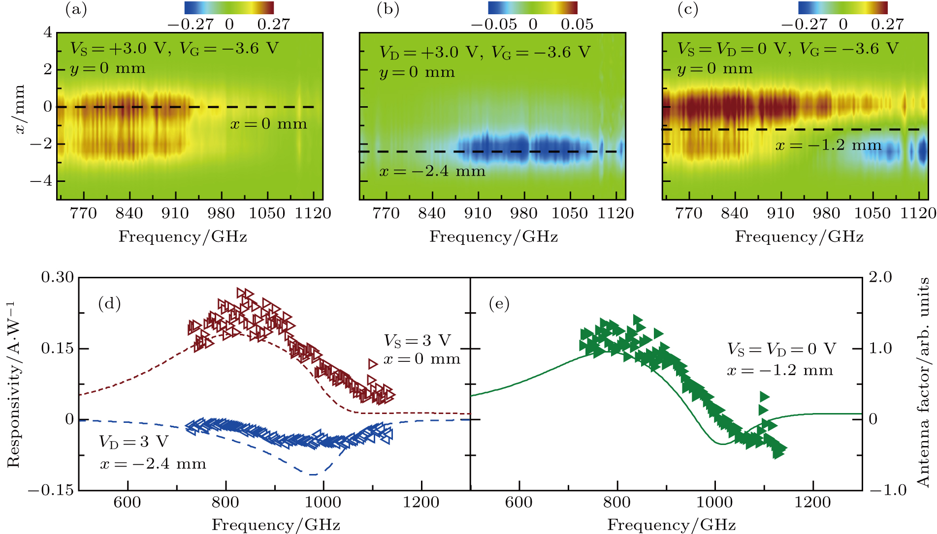
The effect of the three-block antenna and the interplay of the local self-mixing currents in M@S and M@D can also be seen when the frequency is swept. To reveal the frequency response, the detector responsivity is obtained by normalizing the photocurrent with the corresponding terahertz power. With a +3 V bias applied on the source, the responsivity as a function of the frequency and the location in x is plotted in Fig. 4(a). When the frequency is lower than 0.90 THz, a strong and positive photocurrent is observed when the beam is shifted to d-antenna. When the frequency is higher than 0.90 THz, only a very weak positive photocurrent is induced. The detector response to the beam location is more symmetric and the peak frequency is around 0.84 THz. When the +3.0 V bias is applied to the drain, as shown in Fig. 4(b), only a negative photocurrent is observed. The peak frequency is shifted to 0.98 THz. Finally, when no bias is applied and the beam is shifted from d-antenna to s-antenna, both positive and negative photocurrent signals are observed, as shown in Fig. 4(c). The negative current is observed again when the beam is shifted to s-antenna and the frequency is above 0.90 THz. This further confirms the nature of the three-block antenna: self-mixing in M@D is mainly induced by d-antenna and g-antenna placed inline, self-mixing in M@S is instead induced by s-antenna and g-antenna placed in parallel. The different antenna configurations result in the different peak frequencies of the photoresponse in M@S and M@D. Simulation results of the antenna factors in M@S and M@D plotted as short-dashed curve and dashed curve in Fig. 4(d) are in good agreement with the two single traces extracted from Figs. 4(a) and 4(b) at x = 0 mm and x = −2.4 mm, respectively. By extracting a single trace from Fig. 4(c) at x = −1.2 mm, i.e., in a condition close to p3 shown in Fig. 2(a), the observed photocurrent without external bias can be well described by the simulated overall antenna factor (solid curve) taking into account both mixing areas, as shown in Fig. 4(e). In this case, a negative photocurrent is induced when the frequency is above 1.01 THz.
Fig. 4. (a)–(c) Responsivity (in A/W) as a function of the frequency and location x. (d) Responsivity extracted at x = 0 mm in (a) and at x = −2.4 mm in (b). The short-dashed curve and the dashed curve are the simulated antenna factors in M@D and M@S, respectively. (e) Responsivity extracted at x = −1.2 mm in (c). The solid curve is the simulated overall antenna factor.
FET-based terahertz detectors require an inherently asymmetric field distribution under the gate. In our specific three-block antenna design, the asymmetric field distribution is assured by d-antenna and g-antenna. The addition of s-antenna introduces an extra antenna mode which is responsible to the negative photocurrent generated in M@S. When the detector is integrated on a hyperspherical silicon lens, the focused beam spot has a dimension comparable to the antenna size, severe image distortion appears due to the interplay of d-antenna and s-antenna. Although the negative photocurrent can be effectively suppressed by an external positive bias applied on the source, the intensity pattern scanned by the lens-coupled detector exhibits strong dependence on the geometric configuration of the antenna and the lens. Hence, a new antenna design enabling an asymmetric field distribution under the gate while maintaining a symmetric radiation pattern is preferred for power detection and imaging. The following procedures could be taken: 1) remove s-antenna and duplicate g-antenna on the other side of the channel to make a new three-block antenna with higher symmetry in the radiation pattern; 2) replace the hyperspherical lens with a hemispherical or hypo-hemispherical lens so as to make the beam spot slightly larger than the antenna size; 3) bias the detector to suppress the unwanted part of the self-mixing currents. Also, methods of calibrating such integrated detectors should be developed to evaluate the performance in recovering the true intensity pattern of an arbitrary incoming terahertz beam.
4. Conclusion
The photoresponse of an antenna-coupled AlGaN/GaN-HEMT terahertz detector integrated on a silicon lens was examined to reveal the effect of the antenna irradiated by a focused terahertz beam. The integrated detector is sensitive to the location of the incident terahertz wave and does not reflect the intensity pattern truthfully. The s-antenna is found to be responsible to the distortion in intensity pattern. Such artefacts might be commonplace in antenna-coupled FET terahertz detectors especially when the terahertz beam is strongly focused with a dimension comparable to the antenna size. Precautions have to be taken when such detectors are used for imaging. Such artefacts are expected to be eliminated by improving the symmetry in the antenna’s radiation pattern while maintaining the strong asymmetry in the terahertz field distribution under the field-effect gate.
The origin of distorted intensity pattern sensed by a lens and antenna coupled AlGaN/GaN-HEMT terahertz detector*
Project supported by the National Key Research and Development Program of China (Grant No. 2016YFF0100501), the National Natural Science Foundation of China (Grant Nos. 61771466, 61775231, and 61611530708), the Six Talent Peaks Project of Jiangsu Province, China (Grant No. XXRJ-079), the Youth Innovation Promotion Association of Chinese Academy of Sciences (Grant No. 2017372), the Russian Foundation for Basic Research (Grant No. 17-52-53063), and the Natural Science Foundation of Jiangsu Province, China (Grant No. BK20160400).
[Li Xiang1, 2, Sun Jian-Dong1, †, Huang Hong-Juan3, Zhang Zhi-Peng1, Jin Lin1, Sun Yun-Fei4, Popov V V5, Qin Hua1, ‡]


