A simulation study of field plate termination in Ga2O3 Schottky barrier diodes
Project supported by the Research Fund of Low Cost Fabrication of GaN Power Devices and System Integration, China (Grant No. JCYJ20160226192639004), the Research Fund of AlGaN HEMT MEMS Sensor for Work in Extreme Environment, China (Grant No. JCYJ20170412153356899), and the Research Fund of Reliability Mechanism and Circuit Simulation of GaN HEMT, China (Grant No. 2017A050506002).
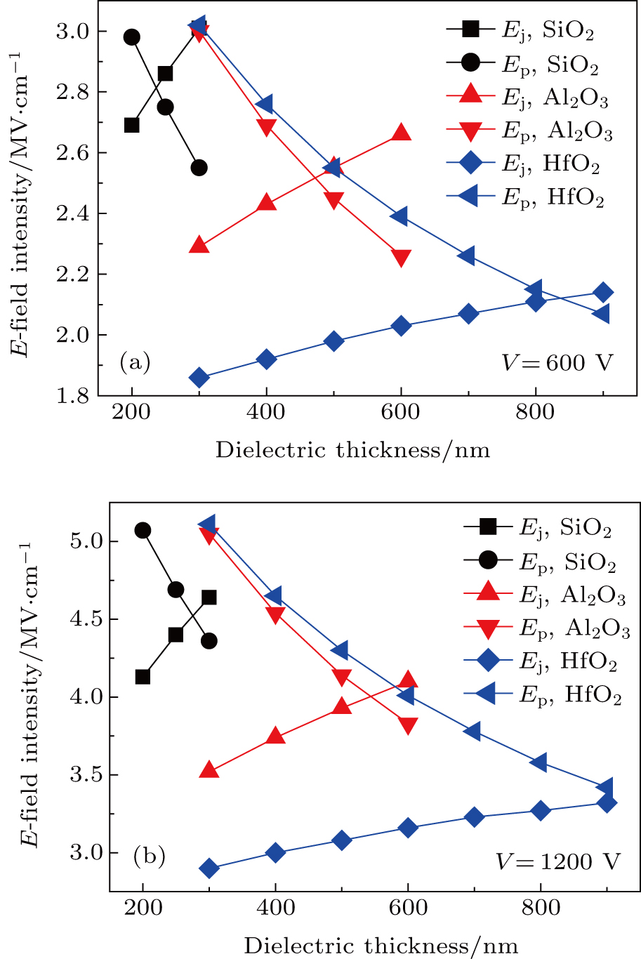
(color online) Plots of Ej and Ep with dielectric thickness for GaN SBDs. The reverse bias voltage is (a) 600 V and (b) 1200 V.
