† Corresponding author. E-mail:
Project supported by the National Key Research and Development Program of China (Grant No. 2016YFB0402504) and the National Nature Science Foundation of China (Grant No. 61435013).
A 16-channel dual tuning wavelength division multiplexer/demultiplexer based on silicon on insulator platform is demonstrated, which is both peak wavelength tunable and output optical power tunable. The wavelength division multiplexer/demultiplexer consists of an arrayed waveguide grating for wavelength division multiplexing/demultiplexing, a heater for peak wavelength tuning and a variable optical attenuator based on p–i–n carrier-injection structure for optical power tuning. The experimental results show that the insertion loss on chip of the device is 3.7dB–5.7 dB and the crosstalk is 7.5 dB–9 dB. For the tunability of the peak wavelength, 1.058-nm wavelength tunability is achieved with 271.2-mW power consumption, and the average modulation efficiency is 3.9244 nm/W; for the tunability of the optical power, the optical power equalization is achieved in all 16 channels, 20-dB attenuation is achieved with 144.07-mW power consumption, and the raise/fall time of VOA is 35 ns/42 ns.
The demand for data is rapidly increasing and, therefore, the further enhancement of information capacity has become a popular topic of research. Dense wavelength division multiplexing (DWDM) technology is a cost-effective solution to expand the capacity of optical interconnects, which offers high bandwidth utilization. Wavelength division multiplexer/demultiplexer is a key component in the DWDM system. Arrayed waveguide gratings (AWGs)[1–3] have been increasingly popular among all devices that can realize wavelength division multiplexing/demultiplexing applications. This is due to the fact that the AWG can realize the multiplexing/demultiplexing function with a large number of channels. The DWDM system requires large channel and small channel spacing, which needs to strictly control the wavelength drift of AWG. Consequently, new methods to realize the precise positioning of AWGs on the ITUT grid have become a necessity.
Silicon photonics,[4–6] which are compatible with the mature complementary metal–oxide semiconductor (CMOS) technology, are a promising solution for future high-speed optical interconnections because they possesses high refractive contrast and the silicon-on-insulator (SOI) based waveguides allow small bent radius, small footprint and, therefore, high level integration of many optical functions[7–14] on a single chip. However, the high refractive contrast of SOI can cause some issues, one of which is its sensitivity to dimensional variation. Take the arrayed waveguide grating (AWG) for instance. Because the AWG is a large device, it is more vulnerable to the kind of dimensional variation and small dimensional variation in its fabrication that will introduce a large peak wavelength shift. Consequently, the methods[15] to stabilize and tune or compensate for optical wavelength drift are of great interest.
In the DWDM system, the optical power of signals with different wavelengths cannot stay the same due to the non-uniformity of the lasers’ output power, the different absorption losses of different signals in their transmission, and the intrinsic non-flat gains of erbium doped amplifier in different channels. The non-uniformities of optical signals with different wavelengths will badly influence the following optical transmission and processing. So methods[16–19] must be taken to ensure that the optical powers of different signals are balanced.
In this paper, a 16-channel SOI-based wavelength division multiplexer/demultiplexer with dual-tunable function is demonstrated, which can realize the wavelength division multiplexing/demultiplexing function, the peak-wavelength tuning function, and the optical power tuning function.
Figure
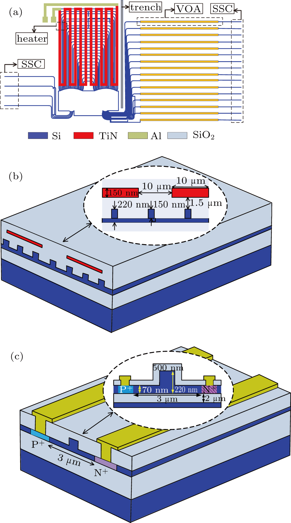 | Fig. 1. (color online) Schematic diagram of (a) top view of wavelength division multiplexer/demultiplexer with dual-tunable function, (b) heater structure, and (c) VOA structure. |
A typical AWG consists of input/output waveguides, input/output slab waveguides, and arrayed waveguides. According to the theory of multi-beam interference, light propagation in the AWG satisfies the grating diffraction equation, as follows:
From Eq. (
| Table 1. Design parameters of silicon nanowire AWG. . |
The heater can be used to compensate for optical wavelength drift. According to the thermo–optic (TO) effect, the peak wavelength shift (Δ λ) arising from the change of temperature (ΔT) can be calculated from Eqs. (
To tune the output optical power of each channel, according to the plasma dispersion effect of silicon, at 1550 nm the index change and the absorption coefficient change can be obtained from the well-known Soref empirical equations:
Figure
As shown in Figs.
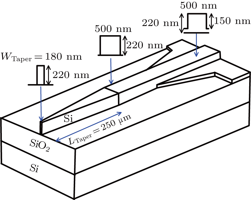
Spot size converters (SSCs) are used to reduce the coupling loss caused by the mode-size mismatch between the input/output fiber and the input/output waveguides of the wavelength division multiplexer, and the diagram of three-dimensional structure of the SSC is shown in Fig.
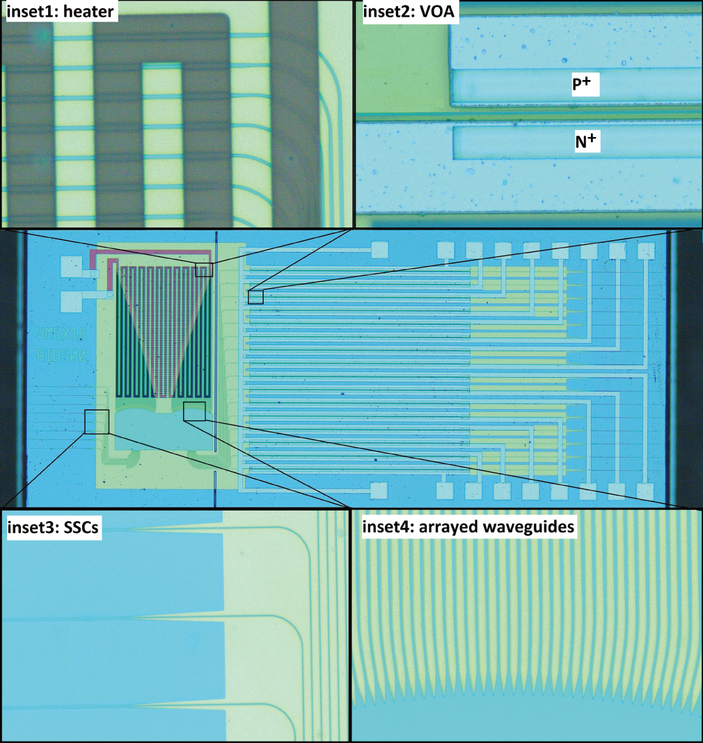
The wavelength division multiplexer/demultiplexer with dual-tunable function was fabricated as follows. First, the rib waveguides was fabricated by deep ultraviolet lithography (DUVL) process and inductively coupled plasma (ICP) etching process. Then, the P+ region and N+ region were formed by boron and phosphorus implantation, respectively, and then the chip was annealed at 1050 °C for 30 min to recrystallize the doping zone. Next, the Si slab was etched to fabricate the channel-type tapers for the SSCs in the input/output waveguide region. A 1.5-μm thick SiO2 layer was then fabricated by plasma-enhanced chemical vapor deposition (PECVD) followed by the fabrication of 150-nm thick TiN as a heater. Finally, SiO2 as the upper cladding layer was deposited by PECVD process and then 1-μm thick Al was deposited to generate the leadwire electrodes and the Al pads. The fabricated device is shown in Fig.
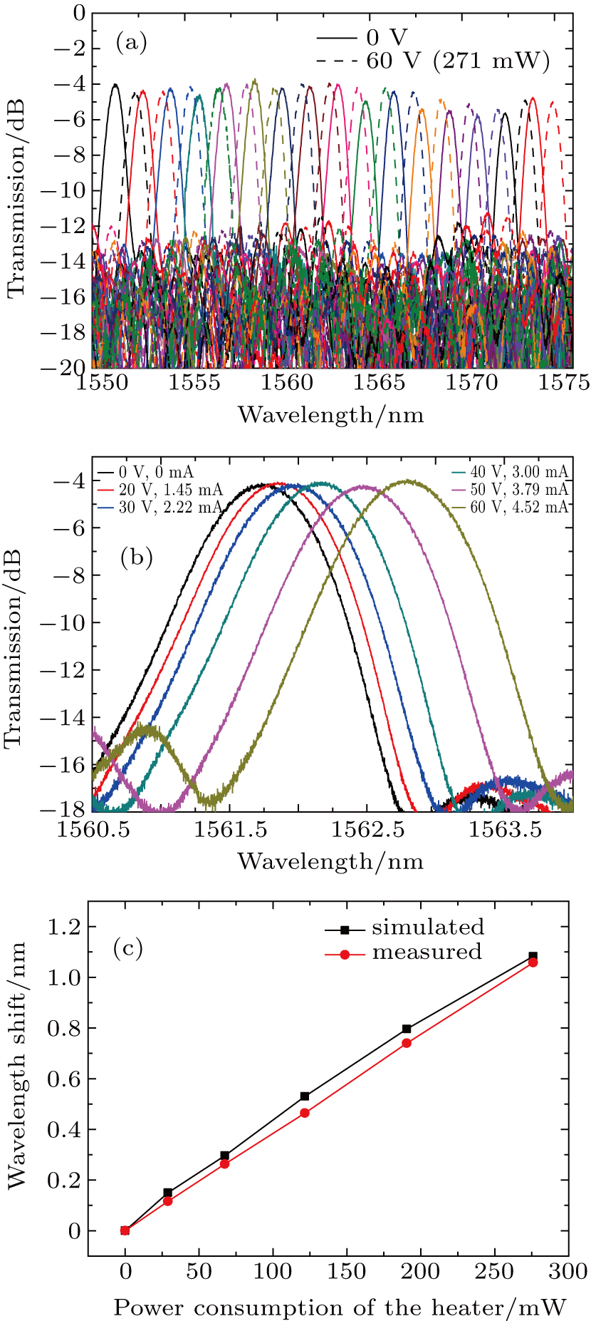
First, the optical property of the AWG before (0 V) and after (60 V) heating were examined as shown in Fig.
| Table 2. Tested results about peak wavelength tunability of the 8th channel. . |
The results of the test of the tunability of the output optical power are shown in Fig.
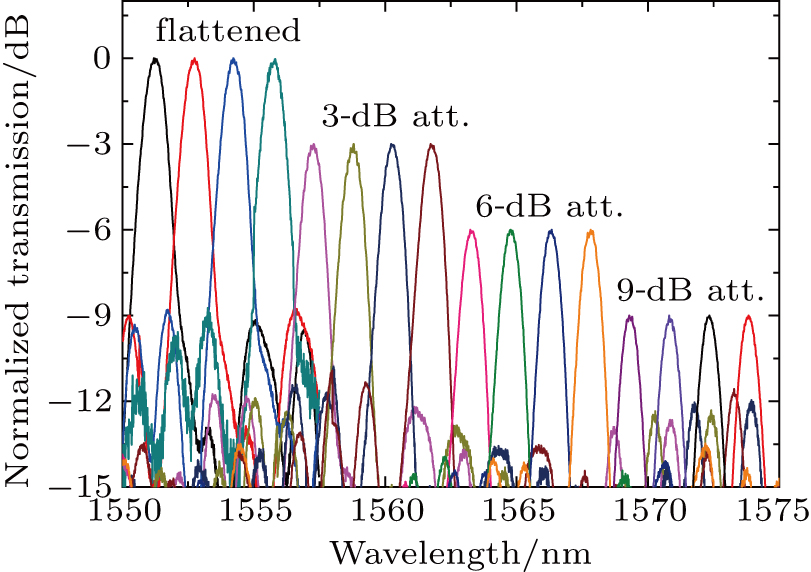 | Fig. 5. (color online) Plots of normalized transmission versus wavelength of wavelength division multiplexer/demultiplexer. |
The performance of the optical power tuning units is then tested, as shown in Figs.
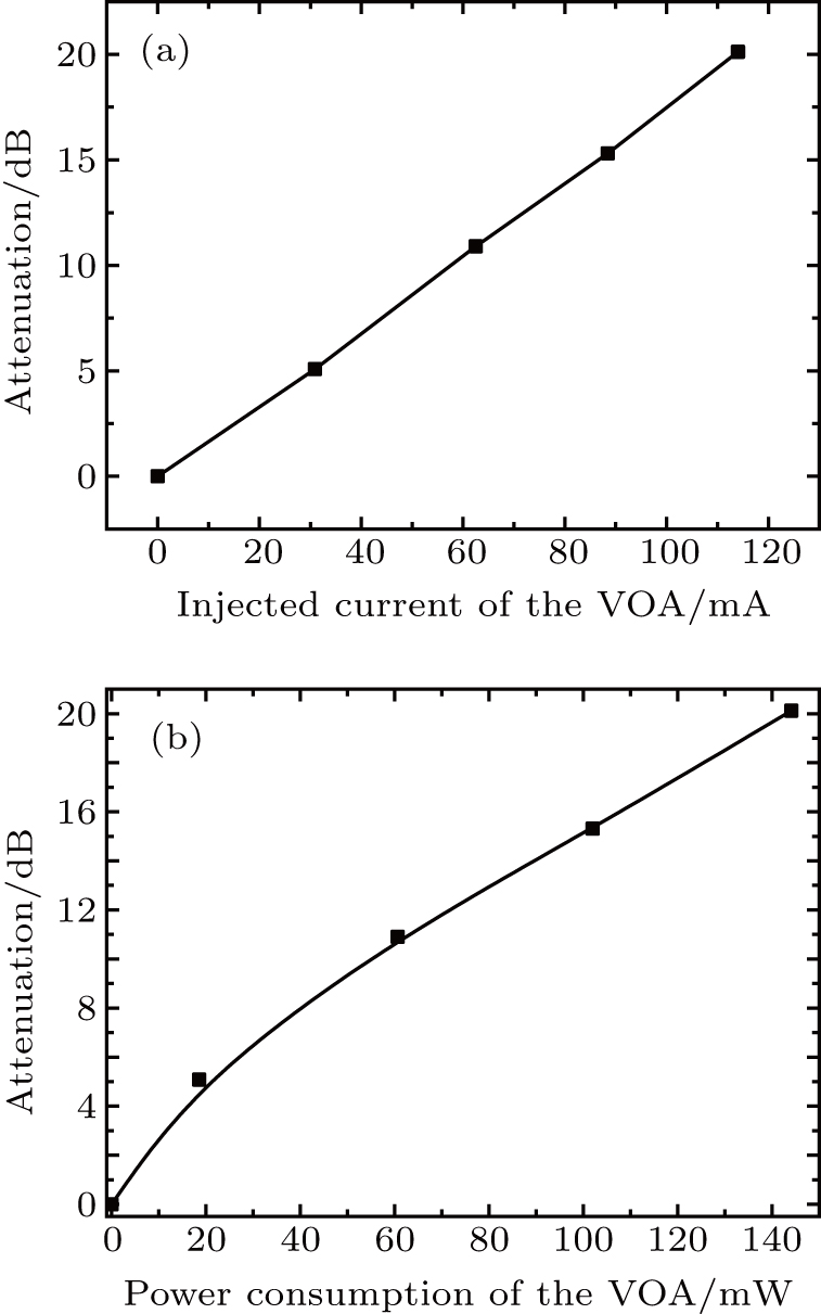 | Fig. 6. Performance of the optical power tuning units, showing dependence of attenuation on (a) injected current and (b) power consumption. |
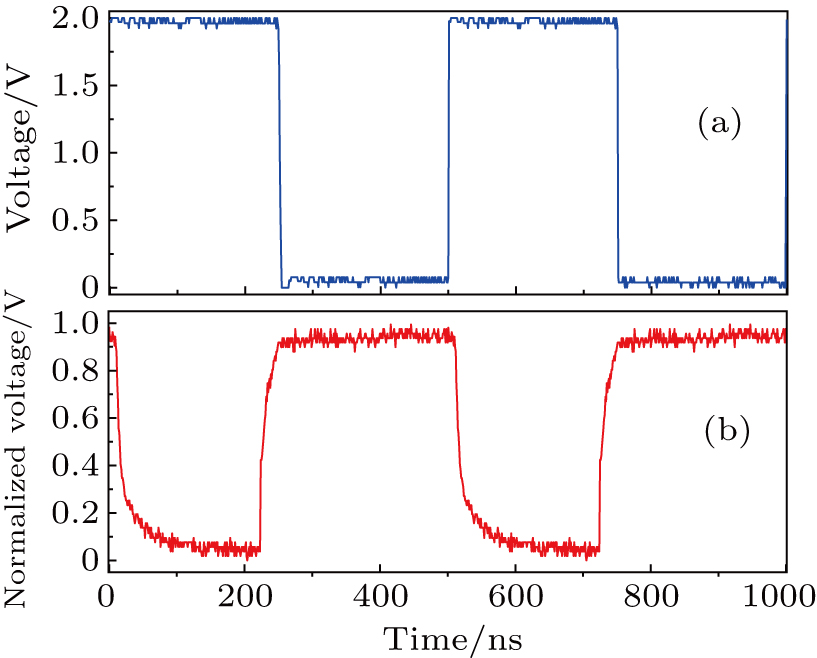 | Fig. 7. (color online) (a) 2-MHz square electrical signal applied to optical power tuning units; (b) measured dynamic response of optical power tuning units. |
| Table 3. The optical power tuning of the wavelength division multiplexer/demultiplexer. . |
In previous work, wavelength tunable AWG based on the SOI[15] has been reported only once, which was fabricated by Nanyang technological university, but its heater structure and fabrication process are relatively complex, including the deposition of five kinds of metal materials, chemical–mechanical polishing process, physical vapor deposition and electrochemical-plating. In the present work, the fabrication process is simplified, which involves the deposition of two kinds of metal materials and metal liftoff process. The modulation efficiency of the device in this work is 3.9 nm/mW, which is in agreement with that in Ref. [15].
Some optical power tunable AWGs have been reported, such as an AWG with VOAs based on SOI with a several-micron top silicon layer,[21] a variable multiplexer/demultiplexer based on silica,[22] and a silica-based AWG with a silicon-nanowire VOA array.[16] However, the silicon-nanowire AWG monolithically integrated with electro-absorption VOA based on SOI with a sub-micron top silicon layer has rarely been reported. Comparisons of the modulation efficiency between our AWG and the typical AWG reported by Nishi et al.[16] are made, which is a silica-based AWG hetero-integrated with a silicon-nanowire VOA array. The power consumption of the device in Ref. [16] is 45.8 mW at 20-dB attenuation, while the power consumption of the device in the present work is 144.07 mW at 20-dB attenuation, which seems to be not satisfactory. However, the modulation length of the VOA in Ref. [16] is 5 mm while ours is 1 mm, and it has been reported that longer modulation length results in smaller power consumption,[23] so the power consumption of our device may be cut down by increasing the modulation length.
Although the wavelength tunable AWG and optical power tuning AWG have been reported, the dual-tuning AWGs with both wavelength tuning and optical power tuning based on SOI have not yet been reported. In this work, we have proposed a dual-tuning AWG with wavelength tuning structure and optical power tuning structure, which can solve the problem of wavelength shift and unbalanced output power of AWG simultaneously.
A 16-channel SOI-based wavelength division multiplexer/demultiplexer, which is both output optical power tunable and peak wavelength tunable, is demonstrated. The wavelength division multiplexer/demultiplexer consists of an arrayed waveguide grating for wavelength division multiplxing/demultiplexing, a VOA based on p–i–n carrier-injection structure for optical power tuning and a heater for peak wavelength tuning. The experimental results show that the insertion loss of the device is 3.7 dB–5.7 dB, the crosstalk is 7.5 dB–9 dB. The methods must be taken to reduce the crosstalk, such as further optimizing the structure between the input/output slab waveguides and the arrayed waveguides. For the tunability of the peak wavelength, 1.058-nm wavelength shift is achieved with 271.2-mW power consumption, and the modulation efficiency is 3.9244 nm/W. For the tunability of the output optical power, the optical power-level control is achieved in all 16 channels and 20-dB attenuation is achieved with power consumption of 144.07 mW. The power consumption can be cut down by appropriately increasing the modulation length of the optical power tuning units or adopting a series structure. The response of the VOA is tested and the rising and falling time of VOA are 35 ns and 42 ns, respectively.
| [1] | |
| [2] | |
| [3] | |
| [4] | |
| [5] | |
| [6] | |
| [7] | |
| [8] | |
| [9] | |
| [10] | |
| [11] | |
| [12] | |
| [13] | |
| [14] | |
| [15] | |
| [16] | |
| [17] | |
| [18] | |
| [19] | |
| [20] | |
| [21] | |
| [22] | |
| [23] |


