† Corresponding author. E-mail:
Project supported by Yifang Wangʼs Science Studio of the Ten Thousand Talents Project, China.
This paper presents the first phase of design, analysis, and simulation for the klystron coaxial radio frequency (RF) output window. This study is motivated by 800 kW continuous wave (CW), 650 MHz klystrons for the future plan of circular electron–positron collider (CEPC) project. The RF window which is used in the klystron output section has a function to separate the klystron from the inner vacuum side to the outside, and high RF power propagates through the window with small power dissipation. Therefore, the window is a key component for the high power klystron. However, it is vulnerable to the high thermal stress and multipacting, so this paper presents the window design and analysis for these problems. The microwave design has been performed by using the computer simulation technology (CST) microwave studio and the return loss of the window has been established to be less than −90 dB. The multipacting simulation of the window has been carried out using MultiPac and CST particles studio. Through the multipacting analysis, it is shown that with thin coating of TiN, the multipacting effect has been suppressed effectively on the ceramic surface. The thermal analysis is carried out using ANSYS code and the temperature of alumina ceramic is lower than 310 K with water cooling. The design result successfully meets the requirement of the CEPC 650 MHz klystron. The manufacturing and high power test plan are also described in this paper.
The Institute of High Energy Physics (IHEP), Chinese Academy of Sciences (CAS), has proposed a future plan of circular electron–positron collider (CEPC) in China,[1] which will be the biggest electron–positron collider in the world. Klystron is a critical component for an efficient and reliable operation of accelerator. As radio frequency (RF) power sources, 192 or even more high efficiency klystrons with a frequency of 650 MHz and a continuous wave (CW) output power of 800 kW are required. These klystrons are expected to be designed at IHEP and manufactured domestically in China. The specifications of CEPC klystron are listed in Table
| Table 1.
CEPC klystron design parameters. . |
For the success of CEPC, the stable operation of klystrons is important, and the RF window used in the klystron is one of its key components. The RF output window is a critical part to transmit high RF power from klystron vacuum side to the external atmosphere with low power dissipation and no breakdown. For window design, it must have a capability of holding the klystron under pressure such as 10−7 Pa, and the good impedance matching is necessary. Furthermore, high power handling capability, excellent mechanical strength, uniform thermal distribution, and low probability of multipacting for ceramic window are required.
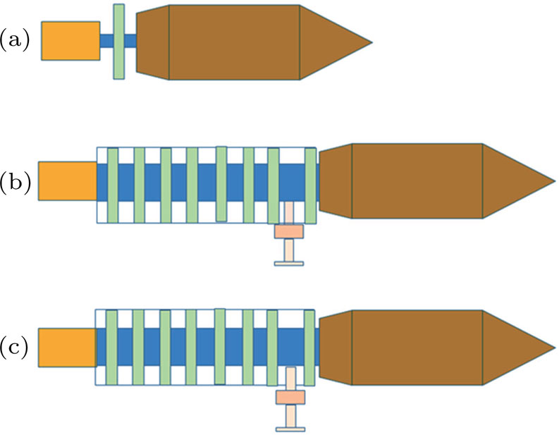
Since it is the first time to design and manufacture such a high power klystron with a coaxial window at IHEP, a project team was formed to start the analysis and simulation. We made a strategy to manufacture a reusable klystron and RF window and proceeded one by one as shown in Fig.
WR1500 (381 mm × 190.5 mm) waveguide is used for transmitting the 650 MHz RF power from klystron to accelerator, but it is difficult to use the pillbox window with rectangular waveguide for the klystron output cavity because of its big size. The interference between the waveguide and the coil for the klystron is severe. The pillbox window has a difficulty in efficiently cooling the center of large aperture ceramic, and then the high temperature may result in a thermal stress that may cause ceramic failure.
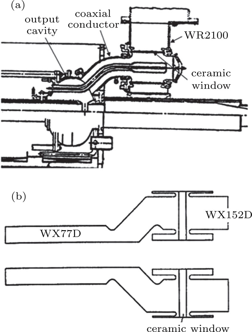
Therefore, we use the coaxial structure coupling to the output cavity and then transfer the power to the WR1500 waveguide. There are three types of coaxial windows which are frequently employed in high power klystron, namely, (i) the cylindrical ceramic window coupling to the rectangular waveguide, (ii) the coaxial window with a choke structure in the inner and outer conductors, and (iii) the simple coaxial window having a hump structure. Type (i) shown in Fig.
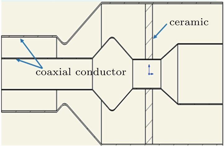
A schematic of the CEPC 650 MHz klystron window is shown in Fig.
To have a good impedance matching, the geometrical design of the window is performed by CST microwave studio code. From the operational requirement, the voltage standing wave ratio (VSWR) of the window is lower than 1.05, and it corresponds to S11 lower than −32.3 dB. After the optimization of the geometrical parameters, we obtain −90 dB for S11 at the operation frequency and less than −30 dB at ±50 MHz bandwidth as shown in Fig.
In order to investigate the mechanical tolerance, we investigate the dimension variation from the optimum value and evaluate the S-parameter and bandwidths. The parameter sensitivity analysis shows that for a ±0.3 mm change in diameter for most of the window components, S11 is changed from −90 dB to −60 dB at 650 MHz, and less than −30 dB at ±50 MHz bandwidth is also obtained. This is achievable and not difficult. The most sensitive parameter is the ceramic thickness, and S11 is changed from −90 dB to −45 dB at 650 MHz for a ±0.2 mm variation. Concerning the ceramic, a purity of 99.5% gives the dielectric constant ε of 10 at the frequency of 650 MHz (provided by Toshiba), and this is used in the simulation. In the high power operation, it is possible that the ceramic temperature goes high, which changes ε from 10 to 9.9, resulting in the small change of the performance.
Besides the usual microwave design of the window, we should pay attention to the window cooling for two reasons. The first reason is that cooling the coaxial coupler or window is not easy, especially for the coaxial inner conductor. The second reason is that a high temperature rise is caused by thermal loss in the inner coaxial line and dielectric loss of the alumina ceramic during the high power operation, which may result in a high thermal stress in ceramic or possibly breaking of the ceramic window. Multipacting on the ceramic surface is another possible source of temperature rise. In this section, the window cooling is analyzed.
Water cooling mechanism is preferred to be considered because of its powerful cooling capability. In CEPC klystron, the power rating of CW klystron reaches 800 kW, and the thermal loss of the window is estimated to be about 800 W. Most of the loss concentrates on the inner conductor, and the heat transferred to the ceramic results in several hundred degrees Celsius. Therefore, only forced air cooling might not be sufficient.
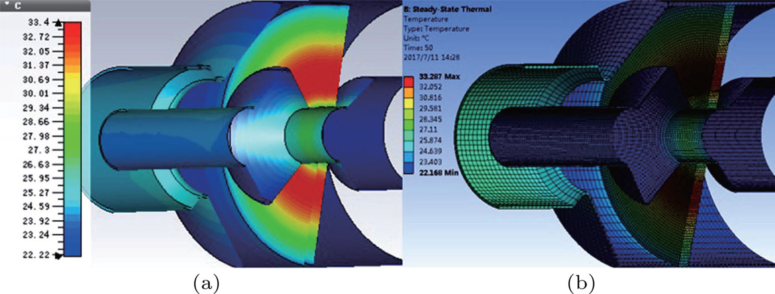
Figure 
The thermal simulation in CST code and ANSYS code is carried out by setting the convective heat transfer coefficient and radiation coefficient. But since the radiation effect is very small in our temperature range, it is sufficient to consider the thermal convection.[11]
The Reynolds number Re is given by
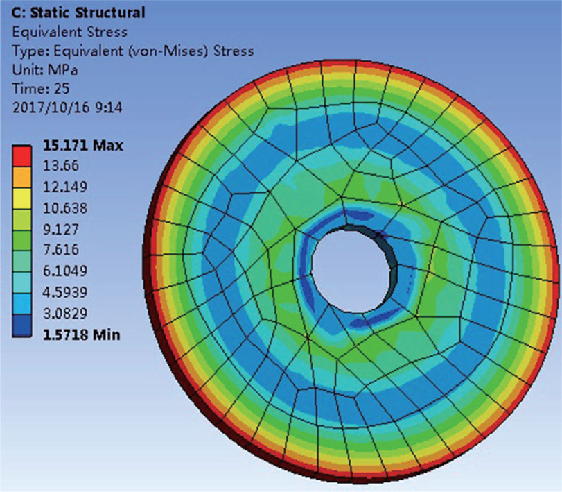
The thermal simulation results in both codes agree well. Figure
The destruction of klystron output ceramic windows is frequently caused by multipacting or surface discharge.[12] Multipacting directly results in surface local overheating of alumina ceramic and ceramic cracking or pinhole, leading to the vacuum leak of the tube. Ceramic window breakdown is one of the most frequent causes of the klystron failure. In this section, multipacting phenomenon is studied and described.
Multipacting is a common phenomenon in the ceramic window and in some cases it causes serious damages. Multipacting is induced by the electrons emitted from the metal surface and the triple junction around the ceramic brazing area. The emitted electrons may collide with the ceramic surface interacting with the RF field, and as a result more electrons are emitted if the secondary electron emission yield (SEY) on the ceramic is high. If this process is repeated, local heating due to this electron multipacting bombardment leads to breakdown. Therefore, avoiding serious multipacting is achieved not only by designing the structure but also by choosing a low SEY ceramic surface.
The ceramic coating with thin coating of TiN (low SEY characteristic) is a popular way to suppress secondary emission. The maximum SEY value can be as high as 5.8 for such high purity alumina ceramic if there is no coating on the ceramic surface. Since TiN is a resistive material and a thick film increases loss, there is an optimum thickness to effectively suppress the secondary electrons. TiN coating thickness is chosen to be about 5 nm from the past experience as described in Ref. [13]. In the case of 5 nm coating, the resistivity of TiN film is very small, so there is little effect on the S-parameter as shown in Fig.
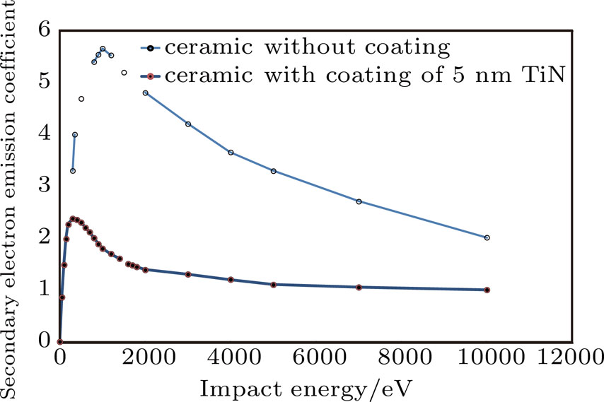 | Fig. 8. (color online) Secondary electron emission coefficient of 99.5% alumina ceramic without and with 5 nm TiN coating. |
From Fig.
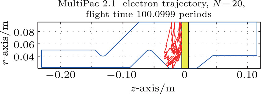
The multipacting simulation is performed using the code MultiPac as shown in Fig.
 | Fig. 9. (color online) Multipacting result in MultiPac version 2.1. (a) Ceramic without coating, and (b) ceramic with 5 nm TiN coating. |
In the case without coating, 
In the case of 5 nm TiN coating in Fig.
 | Fig. 11. (color online) Secondary electron emission on the ceramic (a) without and (b) with 5 nm TiN coating in CST. |
From this result, it is concluded that multipacting may occur without coating, but it is suppressed dramatically with coating.
Since this window is used in the klystron, one side of the window is evacuated. Therefore, two windows connected by the waveguide structure in vacuum are required to be evaluated for their performance similar with the klystron window. The doorknob coupler is designed to achieve water cooling for inner conductor. The pressure inside should be as low as that of klystron, which is about 10−7 Pa. The windows and coupler will be baked before testing.
The hot test includes high power capability of the ceramic window, requiring a proper cooling system with inlet and outlet of water supplied from the doorknob side through double piping structure.
We will increase the power step by step as in the klystron high power operation test. In this test, a solid state amplifier (SSA) with 150 kW CW is available at IHEP. The power transmission test with load is planned followed by the full reflection test by changing the phase. By this test, we can equivalently evaluate the power capability of 600 kW.
The ceramic coating is important; therefore, these windows manufactured by TETD will be coated with 5 nm TiN(O) film on the ceramic surface. The viewport and arc-detector are used to detect multipacting or arcing problems.
We have finished the simulation of the RF coaxial output window to be used in the CEPC 650 MHz, 800 kW CW klystron. We have compared several types of windows and chosen the type (iii) window. The RF design has been fulfilled and the S-parameter has been optimized. The thermal loss and multipacting in ceramic have also been considered in the high power operation. Good window cooling has been successfully introduced after the thermal analysis. After the simulation using CST and MultiPac, it is successfully shown that the suppression of the multipacting with 5 nm TiN coating has been achieved. We have finished the mechanical design and started to manufacture it. The high power test scheme is also described.
The author wants to thank the mechanical design group member Mr. Wang Jianli for his work and suggestions.
| [1] | |
| [2] | |
| [3] | |
| [4] | |
| [5] | |
| [6] | |
| [7] | |
| [8] | |
| [9] | |
| [10] | |
| [11] | |
| [12] | |
| [13] |


