† Corresponding author. E-mail:
Project supported by the National Key Research and Development Program of China (Grant No. 2016YFB0700700), the Science Challenge Project, China (Grant No. TZ20160003), and the National Natural Science Foundation of China (Grant Nos. 51672023, 11474273, 11634003, and U1530401). H. X. D. was also supported by the Youth Innovation Promotion Association of Chinese Academy of Sciences (Grant No. 2017154).
Metal oxides play an essential role in modern optoelectronic devices because they have many unique physical properties such as structure diversity, superb stability in solution, good catalytic activity, and simultaneous high electron conductivity and optical transmission. Therefore, they are widely used in energy-related optoelectronic applications such as photovoltaics and photoelectrochemical (PEC) fuel generation. In this review, we mainly discuss the structure engineering and defect control of oxides for energy applications, especially for transparent conducting oxides (TCOs) and oxide catalysts used for water splitting. We will review our current understanding with an emphasis on the contributions of our previous theoretical modeling, primarily based on density functional theory. In particular, we highlight our previous work: (i) the fundamental principles governing the crystal structures and the electrical and optical behaviors of TCOs; (ii) band structures and defect properties for n-type TCOs; (iii) why p-type TCOs are difficult to achieve; (iv) how to modify the band structure to achieve p-type TCOs or even bipolarly dopable TCOs; (v) the origin of the high-performance of amorphous TCOs; and (vi) band structure engineering of bulk and nano oxides for PEC water splitting. Based on the understanding above, we hope to clarify the key issues and the challenges facing the rational design of novel oxides and propose new and feasible strategies or models to improve the performance of existing oxides or design new oxides that are critical for the development of next-generation energy-related applications.
Metal oxides comprise a group of materials that have many unique structural, electronic, and optical properties suitable for energy applications, for example, the transparent conducting oxides (TCOs) and oxide catalysts are essential materials for photovoltaics[1–3] and hydrogen fuel production,[4–6] respectively. TCOs are usually defined by their high electrical conductivity approaching that of a metallic compound, with high transmission of photons in the visible range of the electromagnetic spectrum. The first TCO thin film was reported by Badeker[7] in 1907, more than 100 years ago, and is based on CdO. Afterwards, more TCOs such as SnO2, In2O3, ZnO, and their alloys have been discovered and utilized in our daily life.[8,9] The most important TCO used today is tin doped indium oxide, In2O3:Sn,[10] typically called indium-tin-oxide or ITO, which is the most used TCO for photovoltaics and flat panel displays.[11]
Although TCO materials are now widely used for optoelectronic applications, many problems still need to be resolved. For example, a TCO is usually a wide band-gap semiconductor that has a relatively high concentration of free electrons (holes) in its conduction (valence) band. These arise either from defects in the material or from extrinsic dopants, such as Al or Ga-doped ZnO, F-doped SnO2, and Sn-doped In2O3. However, so far, all of the commercialized TCO materials are of the n-type, and there is no high-conductivity p-type TCO. Why are most of the well-known TCOs n-type? What kinds of material characteristics are best for n-type TCOs? Why is there no high-conductivity p-type TCO? How can high-level p-type doping in TCOs be achieved? Furthermore, is it possible to have bipolarly dopable TCOs? Furthermore, high carrier concentration can lead to good electrical conductivity but can also cause intra band optical absorption and reflection in both the visible and infrared portions of the light spectrum. How should electrical conductivity and optical transmittance for a high-performance TCO be balanced? How should the extrinsic dopants for n- and p-type doping in TCOs be chosen?
For photoelectrochemical (PEC) water splitting, TiO2 is the most studied photocatalyst because it has high chemical stability, strong catalytic activity, correct band-edge alignment, and high photo-generated current with a long carrier lifetime.[4,12,13] However, because it has a large band gap (∼ 3.2 eV), it cannot absorb visible light in the solar spectrum and thus has a poor solar-to-hydrogen conversion efficiency. How can the visible-light absorption be enhanced without decreasing the high efficiency of the hydrogen reduction reaction? How can the hydrogen-production efficiency of nano oxides for PEC water splitting be improved?
In this brief review, we will address the above issues, and present our understanding with an emphasis on the contributions of our theoretical understanding of the band structure engineering and defect control based on density functional theory. This review is organized as follows. Section
Despite the wide usage of TCO materials, the band structures of these common TCOs are still not very well understood. For example, even though In2O3 with bixbyite structure is widely used as a TCO, the nature of its band gap was only recently resolved by a joint experimental and theoretical effort.[14] In this study, we find that the direct electronic band gap of the bulk material is of the order of 2.9 eV (Fig. 
 | Fig. 1. (color online) (a) Crystal structure and (b), (c) calculated band structure and dipole optical transition of In2O3, showing the large disparity between the fundamental and optical band gaps. Cited from Ref. [14]. |
Another puzzling issue for n-type TCOs is the origin of the free electrons in most of the intrinsic TCOs, which is still not fully clear at present. In previous studies, it is generally assumed that defects such as oxygen vacancies should be responsible for the free electrons. However, if this is true, the donor-like oxygen vacancies must lie at rather shallow levels relative to the conduction band to give such high-carrier concentrations. However, there is no underlying physical reason for this to be true. Indeed, some first-principles calculations performed by us and others suggest that this is not the case.[15–18] For example, our calculated (0/2+) ionization energies of oxygen vacancies in ZnO, SnO2, and In2O3 are 1.15 eV, 0.73 eV, and 0.57 eV, respectively, below the CBM.[15] All of them are very large so the vacancies are hard to ionize and produce enough free carriers at the room temperature. There are also proposals that cation interstitials such as Sni in SnO2 may be responsible for n-type doping in TCOs. However, consensus has not been reached on the origin of n-type doping in TCOs. Therefore, further studies are needed to understand the roles of defects and impurities in introducing carriers to the intrinsic TCOs.
In many cases, the intrinsic defects cannot produce a high enough concentration of electrons, as with most semiconductors, therefore, we may have to use extrinsic dopants to introduce carriers. There is a question about whether we should dope on cation sites or anion sites when extrinsic doping is used to produce better n-type conductivity in the TCOs. It is commonly believed that because the CBM (VBM) states are derived from cation (anion) atoms, doping on anion (cation) sites has less perturbation on the CBM (VBM), so they are expected to produce shallow donor (acceptor) levels. That is why F substitution on the anion O site (FO) has higher electrical conductivity than Sb substitution on the cation Sn site (SbSn) in SnO2. However, for ZnO, the experimental results show that the rule is invalid.[19] It is found that FO produces lower conductivity than Al substitution on the cation Zn site
(AlZn). By analysing the wavefunction characters of the conduction band edge states, we find that this is because for more ionic oxides such as ZnO, the CBM state actually contains a considerable amount of anion O s orbitals and thus anion site doping can cause larger perturbation of the CBM than the cation site doping, and, therefore, give rise to deeper donor levels,[20] as shown in Fig.
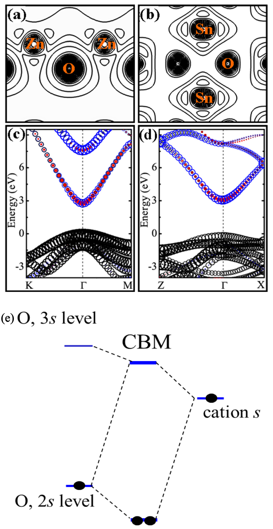 | Fig. 2. (color online) Charge densities of CBM for (a) ZnO and (b) SnO2. Projected band structures near the CBM for (c) ZnO and (d) SnO2. CBM states that are from cation (anion) s states are indicated by blue open circles (red filled circles), while VBM states that are from anion p states are indicated by black open circles. The size of the circle indicates the relative magnitude of the contribution, and the Fermi energy is set to zero. (e) Schematic plot of the band coupling model of ZnO. Cited from Ref. [20]. |
There are some interesting observations on the behavior of TCOs. One of the most obvious observations is that all the dominant TCOs currently used in applications are n-type metal oxides formed from closed-shell large size ns0 cations such as Sn4+, In3+, and Cd2+. The p-type doping in oxides is very difficult. To understand this puzzling phenomenon, we have to review the concept of the so called doping limit rule. In general, there are three main factors that could cause the doping limit in a semiconductor material:[21–24] (i) the desirable dopants have limited solubility; (ii) the desirable dopants have sufficient solubility, but they produce deep levels, which are not ionized at working temperatures; and (iii) there is spontaneous formation of compensating defects. The first factor depends highly on the selected dopants and growth conditions. The second factor only depends on the selected dopants. Thus, these two factors can sometimes be suppressed by carefully selecting appropriate dopants and controlling the growth conditions. The third factor is an intrinsic problem for semiconductors; thus, it is the most difficult problem to overcome, especially for wide band gap (WBG) semiconductors. This is because in forming defects one needs to exchange atoms and/or electrons with certain energies (chemical potentials), so the formation energy of charged compensating defects ΔHf(α, q) = ΔE(α, q) + Σniμi + qEF depends linearly on the position of the Fermi level EF. When a semiconductor is doped, the Fermi level shifts, which can lead to spontaneous formation of the compensating charged defects. For example, when a semiconductor is doped p-type, EF moves close to the VBM. In this case, the formation energy of the charged donor defects decreases because they will donate their electrons to the Fermi reservoir (Fig. 
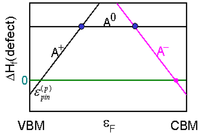 | Fig. 3. (color online) Schematic plot of the dependence of the formation energy of charged defects on the Fermi energy position. The p-type pinning energy  |
With the understanding above, we can now understand why oxides such as CdO, In2O3, SnO2, and Cd2SnO4, etc. can easily be doped n-type, but not p-type. The common electronic characteristic of the above n-type TCO materials is that they have a spatially delocalized, low energy, and low effective mass antibonding CBM state with primarily metal s and oxygen s orbitals. Such a state is achieved with oxides formed from large-size closed-shell ns0 metal ions such as Cd2+, In3+, and Sn4+. Because these metal ions have large sizes, the antibonding state has a lower energy, which is further assisted by the large oxygen s component in these more ionic compounds.[20] According to the doping limit rule, compounds with low CBM are easy to dope n-type. On the other hand, the VBM states of the oxides usually have primarily oxygen p characteristics. Because the oxygen p orbital has very low energy (Fig.
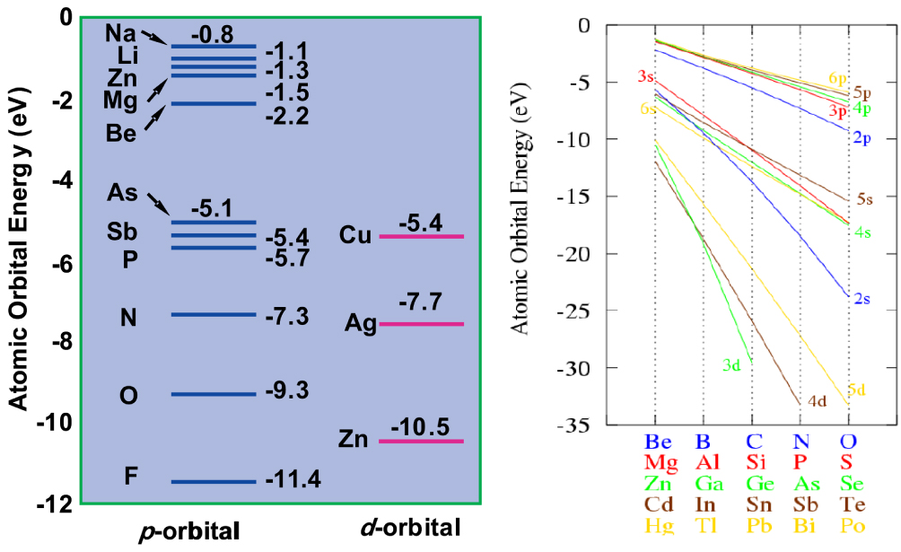 | Fig. 4. (color online) Atomic orbital energies of elements showing that O 2p state has very low energy due to the high electronegativity of oxygen, whereas Cu 3d orbital has much higher energy than O 2p orbital. Cited from Ref. [25]. |
Our understanding of TCOs suggests that a good n-type TCO should have a small fundamental band gap caused by low CBM (i.e., it should contain large cations), but also a large optical band gap due to forbidden band edge transition (i.e., it should have a crystal structure with inversion symmetry and large p–d coupling). To avoid the intra-conduction band optical transition for heavily doped n-type TCOs, the separation between the first and the second conduction bands should also be large (i.e., the material should have large ionicity). On the other hand, to achieve p-type doping of oxides, one has to increase the VBM energy of the oxides. One of the principal approaches is to include a metal with filled low binding energy states at the top of the valence band, such as (n − 1)d10ns0 Cu1+. This is because the Cu d state has much higher energy than O p orbital energy (Fig.
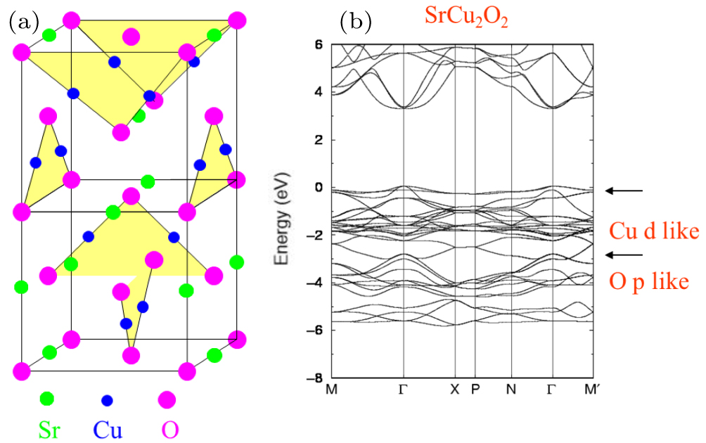 | Fig. 5. (color online) (a) Crystal structure and (b) band structure of SrCu2O2. Because the Cu d band has much higher energy than the O p orbital energy, the VBM energy of the Cu compound is much higher than that of conventional oxides, so it is easier to dope p-type. Cited from Ref. [32]. |
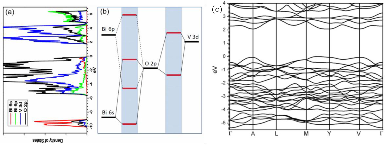 | Fig. 6. (color online) (a), (b) Density of states and (c) electronic band structure of BiVO4 showing that due to the Bi 6s and O 2p interaction, the VBM state is pushed up in energy and becomes more delocalized, so it is easier to dope p-type. Cited from Ref. [34]. |
Our discussion above suggests that according to the doping limit rule, a semiconductor with large band gap can be doped only one type or none under equilibrium thermodynamic growth conditions, because a wide band gap material either has a low VBM or a high CBM or both. Therefore, bipolar doping, that is, doping a material both p-type and n-type, in a WBG material is not possible. In that case, can we still obtain a bipolarly dopable transparent semiconductor? The answer is ‘yes’ if we can have a material like CuInO2.[35] This material contains Cu, thus has a high VBM. It also contains large cation In, so it has a low CBM, so it has a small band gap and can be doped both p- and n-type. However, CuInO2 has a delafossite structure with an inversion symmetry, and the optical transition between the band edge states is zero. Therefore, it can still have good transparency because it has a large optical band gap (Fig.
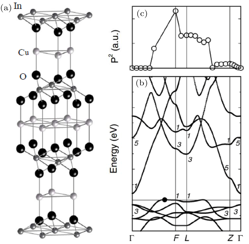 | Fig. 7. (a) Crystal structure, (b) band structure, and (c) dipole transition matrix elements (P2) as a function of wavevector for CuInO2. Cited from Ref. [35]. |
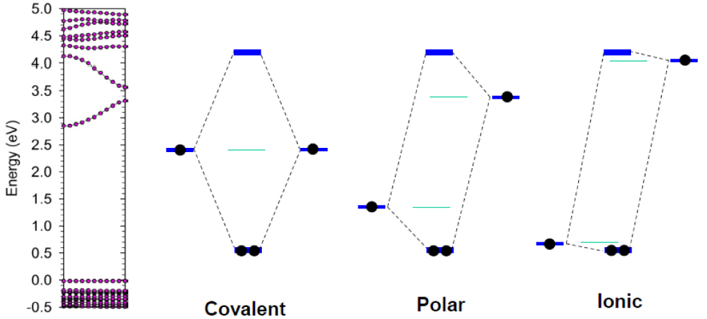
Another interesting observation is that many TCOs can easily form an amorphous phase,[8,36–38] especially during low temperature growth. However, unlike in covalent semiconductors where amorphization can lead to detrimental effects on their electrical conductivity,[39] for many TCOs conductivity is not much affected by amorphization.[36] This is because for ionic amorphous oxides, the defect states induced by amorphization are shallow, so they are not detrimental to the carrier transport.[40] The essential physics of these processes can be captured in a band coupling mechanism based on the energies of the atomic orbitals involved (Fig.
Photoelectrochemical water splitting is a promising process to produce hydrogen fuel with an effective photocatalyst for dissociating water into hydrogen and oxygen by absorbing solar energy.[4,41,42] In this process, the big challenge is the search for an appropriate high-efficiency photocatalyst that should simultaneously meet the following material property criteria: (i) structural stability in water; (ii) consisting of earth-abundant elements with low cost; (iii) appropriate band gap (1.7–2.2 eV); (iv) correct band-edge alignment that straddles the water redox potential levels; (v) high catalytic activity. So far, none of the common semiconductors meet all of these criteria. Anatase TiO2 is the most studied photocatalyst for PEC since it satisfies most of the above criteria. However, it has a low energy conversion efficiency because it has a wide band gap of about 3.2 eV, which is too large to absorb sunlight efficiently, because it absorbs only a small portion of the solar spectrum in the ultraviolet region. Therefore, to improve solar-to-hydrogen conversion efficiency, one needs to modify the band structure of TiO2 by shifting its absorption edge toward the visible light region. Meanwhile, to maintain the high efficiency of the hydrogen reduction reaction, the CBM position should be as high as possible. Based on these considerations, we propose the passivated-codopant model to modify the band edges of TiO2. By identifying atomic wave function characters of the band edge states of TiO2, as well as the chemical potentials of the dopants, we find that the Mo+C passivated codopants can significantly reduce the band gap of TiO2, and simultaneously shift the valence band edge up significantly, while leaving the conduction band edge unchanged,[43] as shown in Fig.
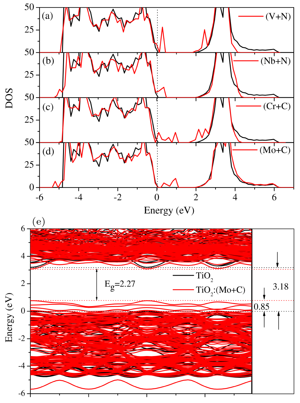 | Fig. 9. (color online) (a)–(d) The LDA-calculated total DOS of undoped TiO2 and (V+N), (Nb+N), (Cr+C), and (Mo+C)-codoped TiO2. (e) The band-structure comparison between pure TiO2 and TiO2: (Mo+C) calculated with LDA+U. Cited from Ref. [43]. |
The modified band-edges and band gaps of TiO2 depend sensitively on the dopant or alloy concentration. In previous studies, this effect is not carefully investigated. To check this effect, we compare the band offsets for TiO2 and TiO2 alloyed with various passivated donor–acceptor combinations in the low- and high-concentration regimes,[45] as shown in Figs.
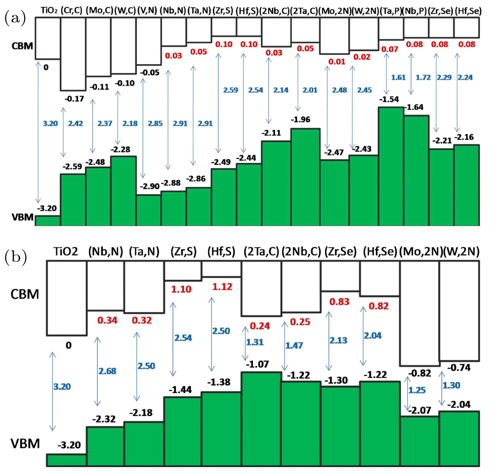 | Fig. 10. (color online) The band offsets (at the Г point) for TiO2 and TiO2 alloyed with various passivated donor–acceptor combinations in the (a) low-concentration and (b) high-concentration regimes. The CBM of pure TiO2 is set to zero as the reference. Cited from Ref. [45]. |
Nanostructured semiconductors are usually more suitable for photocatalysis applications because they have a large surface-to-volume ratio that can significantly improve the catalytic reaction rate.[5,46,47] However, nanostructured oxides are often believed to be inadequate for photocatalysis applications because their band gaps are too large due to the quantum confinement effect, and they fail to absorb a significant fraction of visible light. Can the band gap of nano oxides be reduced, and be made even smaller than that of their bulk counterparts? On the other hand, in theoretical studies of thin film and nanostructured oxides, pseudo-hydrogen (PH) is widely used to passivate the surface dangling bonds to reduce surface states.[48,49] However, in reality, PH does not exist in the real world, and only the real-hydrogen (RH) atom is available. Through systematically comparing the differences between PH-passivated and RH-passivated oxide surfaces and nano structures, we show that, unlike PH passivation, which always increases the band gap with respect to the bulk value, RH passivation will produce the gap states and largely reduce the band gap of the nanostructured oxides.[50] For the nano TiO2, this effect leads to an effective reduction of the band gap (Fig.
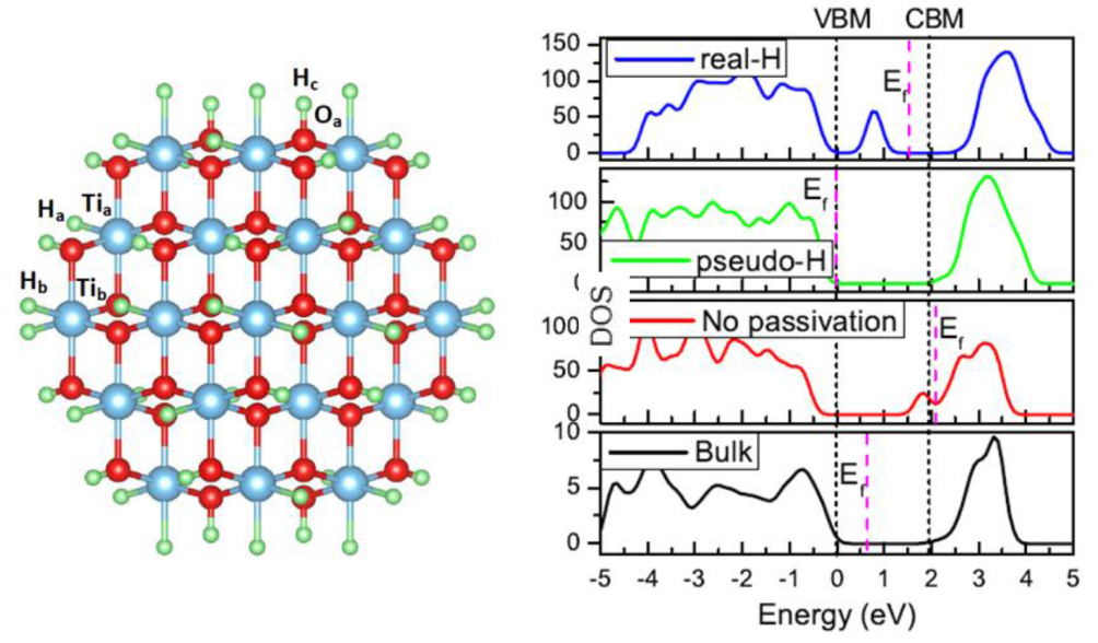 | Fig. 11. (color online) The calculated total DOS of bulk TiO2, no-passivation, RH- and RH-passivated TiO2 quantum dots, respectively. The VBM of bulk TiO2 is set to zero as the reference. Cited from Ref. [50]. |
In this paper, we have reviewed the main issues and difficulties related to the band structures and defect limitations of oxides for energy applications. Specifically, we discuss criteria on the band structures for excellent n-type TCOs, and the principles of choosing the extrinsic dopants for n-type TCOs. Then, we explain the origin of the difficulty in performing p-type doping on oxides, and propose some solutions overcoming the p-type doping bottleneck in oxides. We also propose material characteristics to achieve bipolar doping of TCOs. Moreover, we demonstrate the microscopic origin of the excellent conductivity and optical transparency of amorphous oxides. Finally, taking TiO2 as example, we show how band structure engineering can be used to significantly enhance the photocatalytic water-splitting efficiency of bulk and nano TiO2. We believe that the above understanding will be helpful in engineering material properties of oxides for future energy applications.
Even though remarkable achievements have been made in the development of oxides for energy-related applications, there are still many challenges in this field. For n-type TCOs, although ITO has remarkable material properties, one still needs to further improve its transparency and electrical conductivity. Moreover, due to the scarcity and high price of In, it is desirable to develop and search for new alternatives that are low-cost, non-toxic, and have a performance similar to or even higher than that of ITO. For p-type oxides, because both the doped carrier concentration and mobility are far below the standard for commercial applications, one still needs to develop practical strategies to achieve high-performance p-type conductivity, possibly including non-equilibrium growth methods, transition metal doping, complex doping, multivalence-impurity doping to increase the carrier concentration, and band structure engineering to increase the carrier mobility and optical transparency.
| [1] | |
| [2] | |
| [3] | |
| [4] | |
| [5] | |
| [6] | |
| [7] | |
| [8] | |
| [9] | |
| [10] | |
| [11] | |
| [12] | |
| [13] | |
| [14] | |
| [15] | |
| [16] | |
| [17] | |
| [18] | |
| [19] | |
| [20] | |
| [21] | |
| [22] | |
| [23] | |
| [24] | |
| [25] | |
| [26] | |
| [27] | |
| [28] | |
| [29] | |
| [30] | |
| [31] | |
| [32] | |
| [33] | |
| [34] | |
| [35] | |
| [36] | |
| [37] | |
| [38] | |
| [39] | |
| [40] | |
| [41] | |
| [42] | |
| [43] | |
| [44] | |
| [45] | |
| [46] | |
| [47] | |
| [48] | |
| [49] | |
| [50] |


