Semiconductor photonic crystal laser
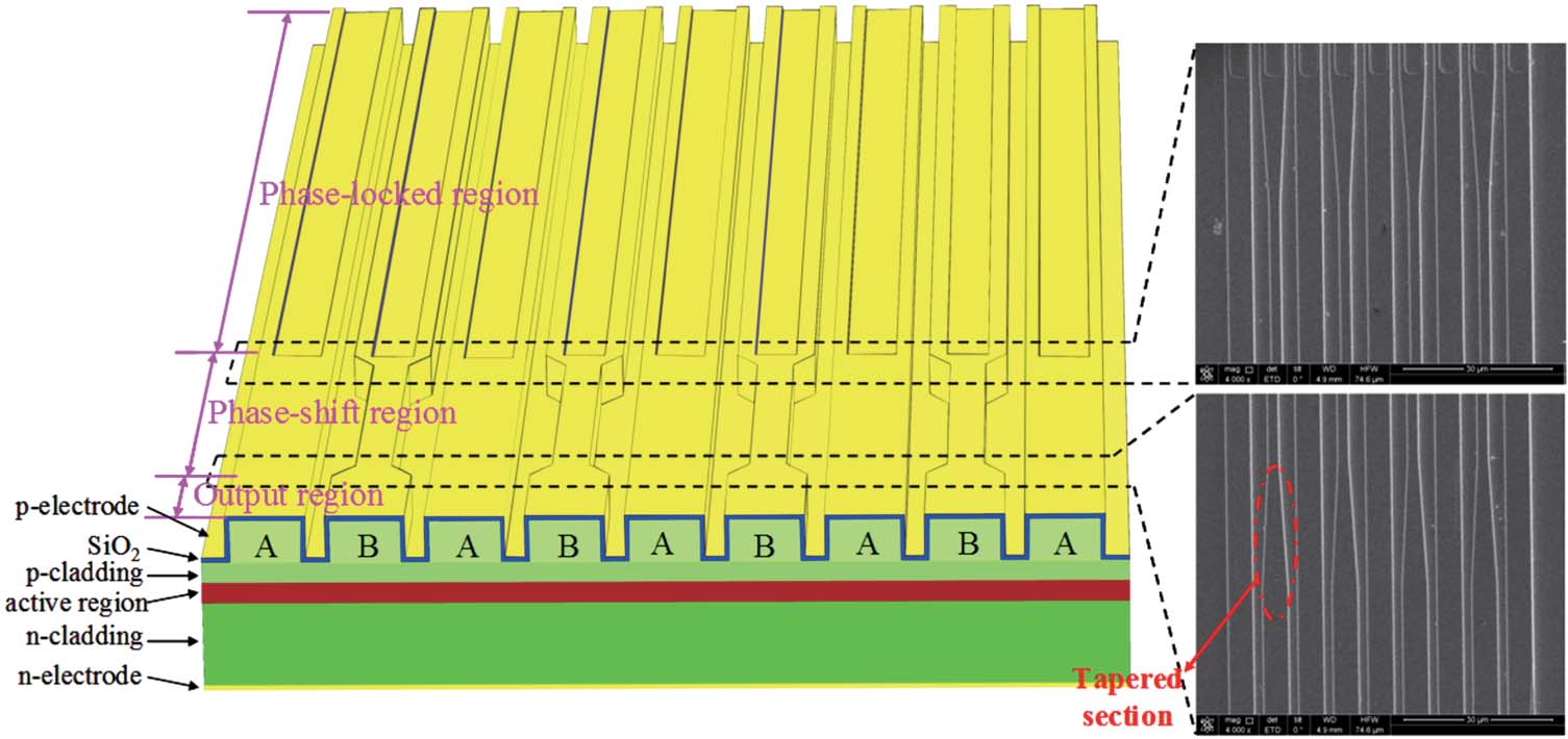
(color online) Schematic of the device’s structure. SEM images (inset) show the zoomed-in view of the tapered sections in the phase-shift region.[
Semiconductor photonic crystal laser |
(color online) Schematic of the device’s structure. SEM images (inset) show the zoomed-in view of the tapered sections in the phase-shift region.[ |
| |