Efficient thermal analysis method for large scale compound semiconductor integrated circuits based on heterojunction bipolar transistor
Yang Shi-Zheng, Lv Hong-Liang, Zhang Yu-Ming, Zhang Yi-Men, Lu Bin, Yan Si-Lu
School of Microelectronics, Xidian University, the State Key Laboratory of Wide Band Gap Semiconductor Technology, Xi’an 710071, China


† Corresponding author. E-mail: hllv@mail.xidian.edu.cn

Project supported by the Advance Research Foundation of China (Grant No. 9140Axxx501), the National Defense Advance Research Project, China (Grant No. 3151xxxx301), the Frontier Innovation Program, China (Grant No. 48xx4), and the 111 Project, China (Grant No. B12026).

Abstract
Abstract

In this paper, an efficient thermal analysis method is presented for large scale compound semiconductor integrated circuits based on a heterojunction bipolar transistor with considering the change of thermal conductivity with temperature. The influence caused by the thermal conductivity can be equivalent to the increment of the local temperature surrounding the individual device. The junction temperature for each device can be efficiently calculated by the combination of the semi-analytic temperature distribution function and the iteration of local temperature with high accuracy, providing a temperature distribution for a full chip. Applying this method to the InP frequency divider chip and the GaAs analog to digital converter chip, the computational results well agree with the results from the simulator COMSOL and the infrared thermal imager respectively. The proposed method can also be applied to thermal analysis in various kinds of semiconductor integrated circuits.

1. Introduction

InGaP/GaAs or InGaAs/InP heterojunction bipolar transistors (HBTs) are widely used in mixed-signal, high-speed, or high-power circuits[14] with the advantages of high cut-off frequency[58] while maintaining high breakdown voltage.[911] Today, with the development of integrated circuits (ICs) and the growth in military and commercial applications, the size of HBT has been scaled down rapidly for higher operating frequency, leading to a huge number of devices integrated in a small chip and a higher current density. Because of the self-heating and thermal coupling effect, the thermal problem becomes more and more serious in HBTs.[1214] With the temperature increasing in a device, the electrical device characteristics could degrade due to the thermal instability,[1517] which reduces the reliability of the circuit seriously.[1820] Therefore, it is of great importance to evaluate the distribution of temperature accurately during the design of integrated circuits.

With the technology of ICs entering into the nanometer domain, the thermal analysis for large ICs faces great challenges. Many improved numerical methods for fast thermal analysis were developed,[2124] in which compact heat transfer equations are solved to characterize the temperature distribution in all parts of the IC chip including the thick substrate based on partitioning an IC chip into many discrete three-dimensional (3D) elements.[25,26] The accuracy of the temperature distribution increases with the number of discrete 3D thermal elements increasing. In this case, the calculation would be significantly time-consuming, which makes it hardly possible to achieve a large scale circuit.

However, the heat source generated by the active layer of each device in an IC is usually located in a thin layer close to the top surface of the IC chip, so only the temperature distribution within the related layer is of interest. For an HBT, the current flows from the emitter junction into the collector junction and the collector junction is at high reverse bias, so the power dissipation is mainly from the collector junction.[27] As a result, the collector junction will be the high-temperature region and the highest temperature will be located in the middle area between the base and collector, which is the so-called junction temperature. It will be easy to obtain the important temperature information of the IC chip with minor calculations if the highest temperature in this area is calculated for each heat source, avoiding a huge quantity of calculations of the numerical methods mentioned above.

In this paper, a semi-analytic temperature superposition method (SATSM) is proposed, based on the principle of superposition of temperature with considering the self-heating effect of the device and the thermal coupling effect between devices. The temperature distribution for the full chip can be easily depicted by calculating the highest temperatures for all devices in a chip with high efficiency and reasonable accuracy. Meanwhile, the temperature dependence of thermal conductivity on the thermal coupling from devices between each other should be considered in implementing the temperature superposition, otherwise, the measured temperature is higher than the calculated temperature and the difference increases with temperature increasing, especially in the high-temperature region.

A more accurate thermal analysis method based on an iterative algorithm, called SATSM-I, is proposed with considering the temperature dependent thermal conductivity. The SATSM-I shows higher accuracy while SATSM exhibits high efficiency and simplicity in calculation. The detailed steps of SATSM and SATSM-I are described in Section 2. The temperature distributions of the InP HBT frequency divider circuit and GaAs HBT analog to digital converter (ADC) chip designed by our research group[28] and calculated by SATSM-I are compared with the results from SATSM, the simulator COMSOL and the infrared thermal imager respectively in Section 3 for verification. Finally, some conclusions are drawn from the present study in Section 4.

2. Temperature distribution calculation procedure

Based on the principle of superposition of temperature, there are three factors to affect the thermal distribution, which include the self-heating effect of the individual device, denoted as , the thermal coupling effect from the devices between each other, named , and the ambient temperature Ta.

Therefore, the SATSM calculation procedure mainly consists of two steps.

Step 1.1 The initial temperature Ta is assigned to each device in the circuit.

Step 1.2 The temperature increments of and of each device are calculated, according to the semi-analytic temperature distribution function for each kind of device, and the junction temperature T of each device can be worked out finally by temperature superposition. The computation process will be done and the final junction temperature T will be output.

In this case, it is very convenient to obtain the temperature distribution of the HBT IC as long as the semi-analytic temperature distribution function for each device is determined. Each kind of device is firstly simulated by using COMSOL, and the semi-analytic function of the temperature distribution is obtained by fitting with MATLAB. Then, the highest temperature of each device will be worked out with the algorithm based on Steps 1.1 and 1.2, which is implemented in MATLAB.

Table 1 shows the thermal conductivities of the semiconductor materials, in which the thermal conductivity of the semiconductor material decreases as temperature increases. In this case, the and will be intensified when local temperature TLo is increased. Thus, the temperature of devices calculated by the superposition of the semi-analytic temperature distribution function will be lower than the actual temperature if the temperature dependence of thermal conductivity is not considered.

Table 1.

Thermal conductivity of semiconductor material.

.

The influence caused by the thermal coupling effect from the adjacent device in a circuit can be equivalent to the change of local temperature TLo. Thus, TLo can be replaced by a slightly higher local temperature , resulting in the re-change of the thermal conductivity of materials. The TLo would approximate well to the actual local temperature by the continuous iteration procedure. Therefore, more accurate junction temperature T of each device can be obtained. Based on the idea above, an efficient thermal analysis method (SATAM-I) is proposed with the following calculation steps.

Step 2.1 The initial Ta and TLo are assigned to each device in the circuit.

Step 2.2 The temperature increments and for each device will be calculated, according to the semi-analytic temperature distribution function for each kind of device, and the junction temperature T of each device can be worked out finally by temperature superposition.

Step 2.3 The new of each device can be obtained according to the relationship between T and TLo.

Step 2.4 The computational process will be done and the final junction temperature T will be output if the relative error between TLo and is less than or equal to the specified iterative precision for all devices in a circuit, otherwise, will be re-assigned to TLo for the corresponding device and the process will be repeated from Step 2.2 until the precision is satisfied.

In order to realize the total computational process to obtain the temperature distribution of the HBT IC, the temperature distribution of each kind of device is first simulated by using COMSOL, and the semi-analytic function of temperature distribution is obtained by fitting with MATLAB, the same as the process made in SATAM. In the following, the GaAs HBTs with four sizes are taken for example to describe the total computational process.

2.1. Semi-analytic temperature distribution function for individual device

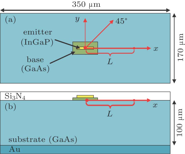
Before making the function fitting for a single GaAs HBT, the model of each kind of device is first set and its temperature distribution is simulated by COMSOL. Figure 1 shows the schematic diagram of a GaAs HBT simulation model. The simulation region is including the backside metallization and passivation layer. For the thermal boundary conditions, the bottom of the model is set to be at different local temperatures and the rest of the boundaries are in natural convection in air. In order to obtain the accurate simulation results, the temperature dependent thermal conductivity is involved as shown in Table 1.

Fig. 1. (color online) Schematic diagram of GaAs HBT simulation model, showing (a) top view and (b) sectional view.

The collector–emitter current flows through the collector-base depletion region with high reverse voltage, resulting in the highest Joule heating. Therefore, heat generation comes from the collector-base depletion region.[30] In order to simplify the model, the power of each device is applied to the interface between the base and collector, which is called the heat source that is assumed to cover the emitter area as shown in Fig. 2. The highest temperature would be located at the center of the heat source, which is called junction temperature.
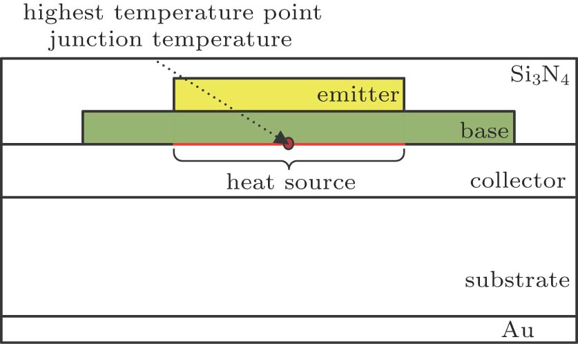
Fig. 2. (color online) Position of the heat source and the highest temperature point in the simulation model.

The is affected by dissipated power p, heat source area s, and local temperature TLo. Thus, is a function of p, s, and TLo and is expressed as

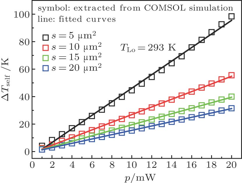
Figure 3 indicates the center temperatures versus power dissipation from 0 to 20 mW for four devices with different emitter areas. It is apparent that the temperature is a linear function of dissipated power p, and can be expressed by an empirical equation (2):

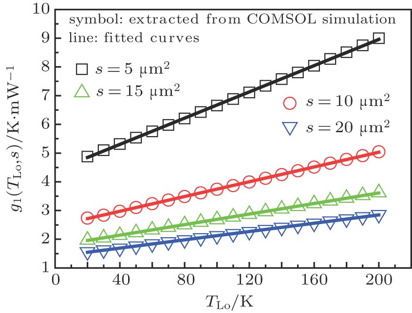
where is a function of and s. The increases linearly with TLo as given in Fig. 4, and can be rewritten as follows:

Fig. 3. (color online) Plots of versus p for different sizes of devices at 293 K.
Fig. 4. (color online) Plots of versus TLo for different sizes of devices.

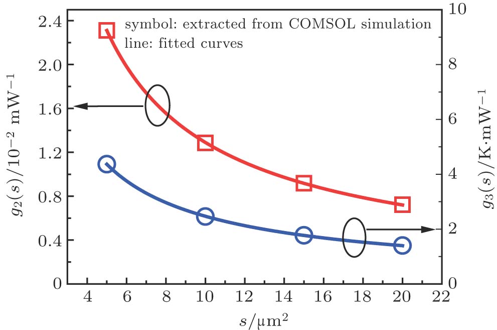
Since and decrease exponentially with s as given in Fig. 5, equation (3) can be rewritten as

where are four constants extracted from the data fitting in Fig. 5.

Fig. 5. (color online) Plots of and versus s.

Then the junction temperature T(i) can be given as follows:

which is the temperature at the center of a single heat source i without the thermal coupling from other heat sources.

Based on the relationship between the junction temperature T(i) and the local temperature in Eq. (5), can be derived and expressed as follows:

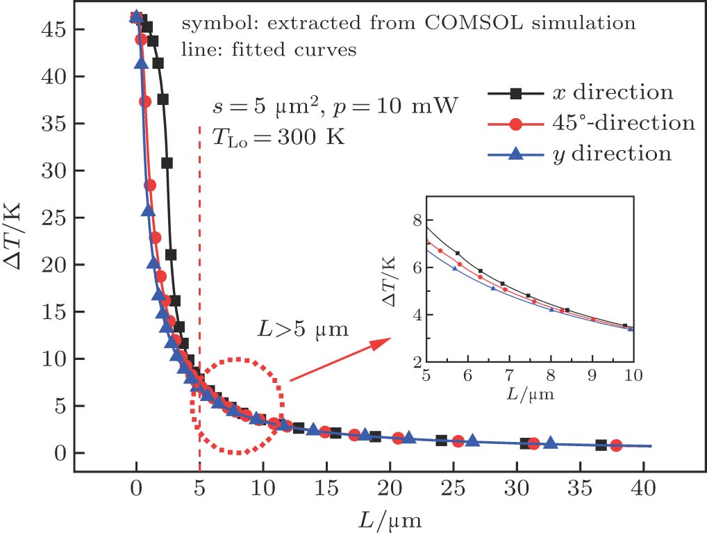
figure 6 illustrates the variations of the temperature increment with distance L from the central point along three directions: x direction, y direction, and 45°-direction in the plane at a power of 10 mW for the device with an emitter area of at 300 K, with the three directions shown in Fig. 1. It is obvious that the temperature differences in the three directions are large within a distance of , and the maximum temperature difference can reach 25 K between the x direction and y direction because of the rectangle emitter.

Fig. 6. (color online) Plots of versus L from the central point along three directions.

Whereas, for the distance larger than , the thermal profile is almost the same in the three directions. In this case, it can be found from the layout of the GaAs HBT ICs that the distance from the center point of the device is at least . Therefore, there is no big difference of the temperature distributions in three directions for expressing the thermal coupling effect and it is reasonable to choose the x-direction in the following calculation. The cut-off distance is adopted for the GaAs HBT technology currently used. For the other types of circuits, the method is also applicable. The difference is that the cut-off distance would decrease to a few nanometers, such as VLSI, where the distance between devices is on the nanoscale.

The temperature increment away from the center point is denoted as . The is a function of the distance L between two devices, p, s, and TLo. Therefore, can be expressed as

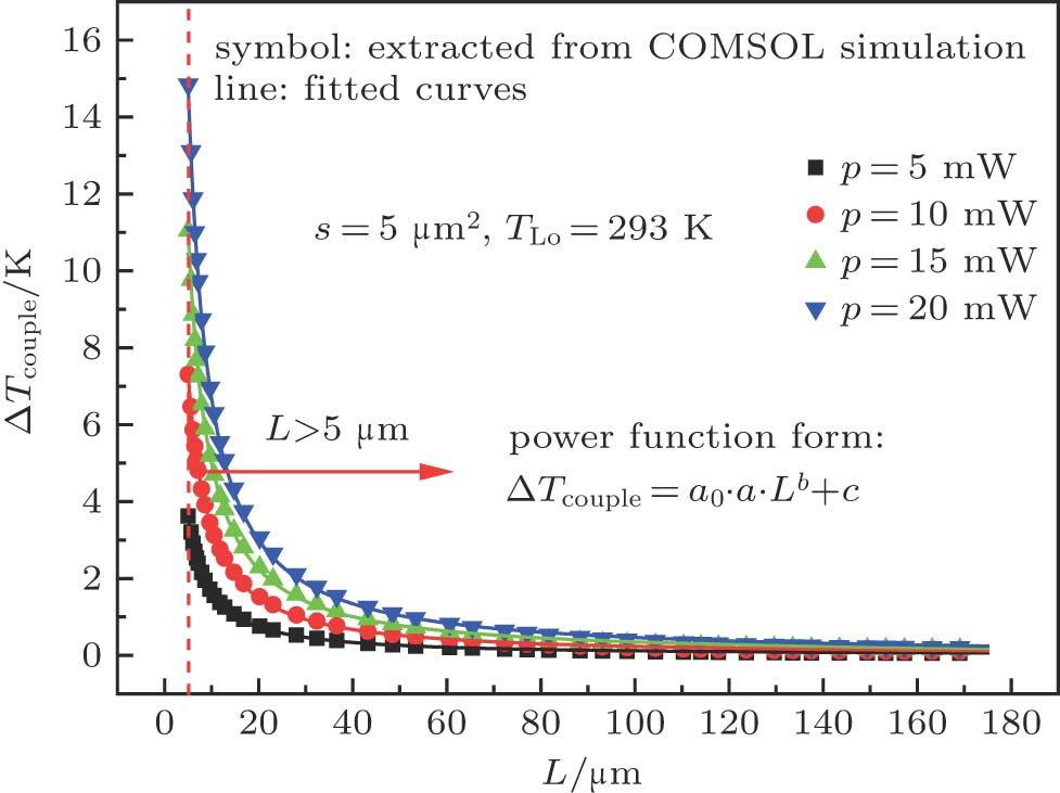
Figure 7 shows the temperature of the device with an emitter area of in the x-direction for four different powers at 293 K. It is clear that the temperature distribution at more than away from the center point exhibits the power function form as expressed below.

where is defined as to express the units of the three above undetermined coefficients a, b, and c conveniently.

Fig. 7. (color online) Temperature distributions in the x direction for different powers.

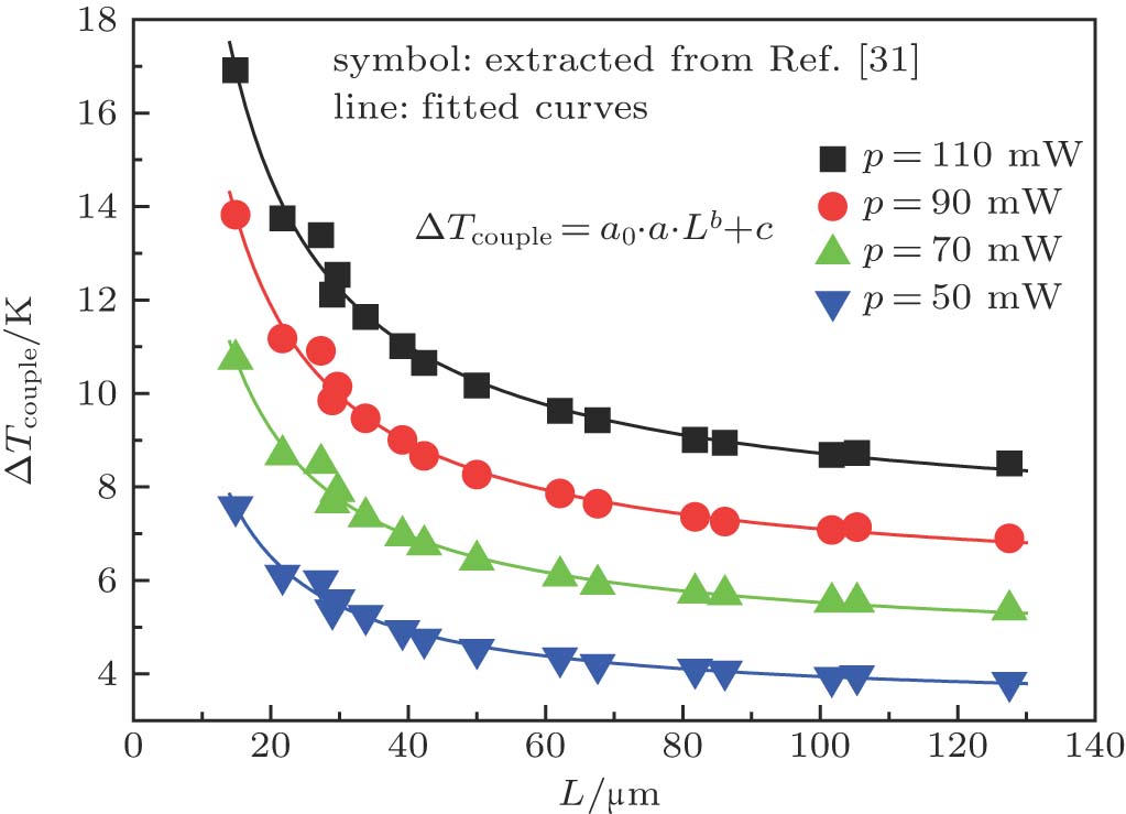
This power function of , i.e., Eq. (8), has been verified.[31] figure 8 shows the temperature increment versus L with power dissipation caused by a resistor as an on-chip heater from 50 to 110 mW in steps of 20 mW, which is measured by p–n diode sensors at 293 K. The fitted curves in the power function form are consistent with the measured data.

Fig. 8. (color online) versus L for different p at 293 K in Ref. [31].

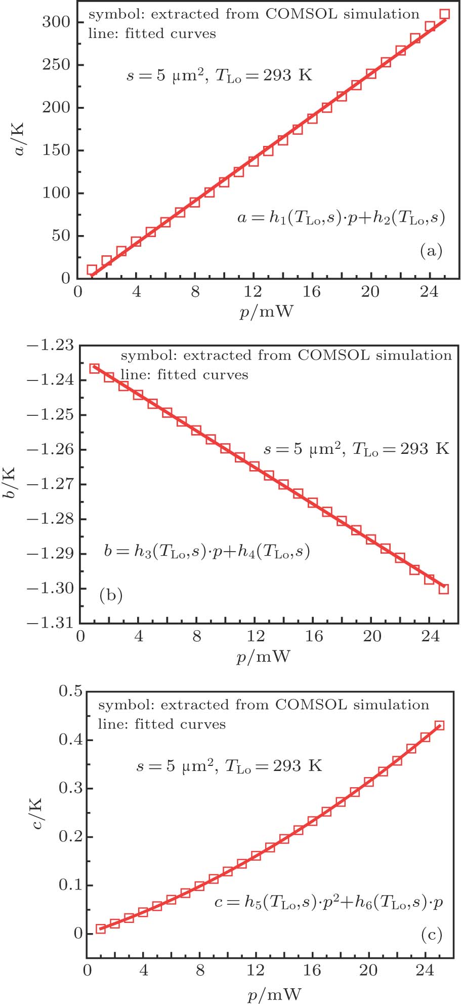
Figure 9 shows the relationship of a, b, and c with the dissipated power p for the device with an emitter area of at 293 K. The a, b, and c can be expressed by Eqs. (9), (10), and (11), respectively,

Fig. 9. (color online) Relationships of a, b, and c with p.

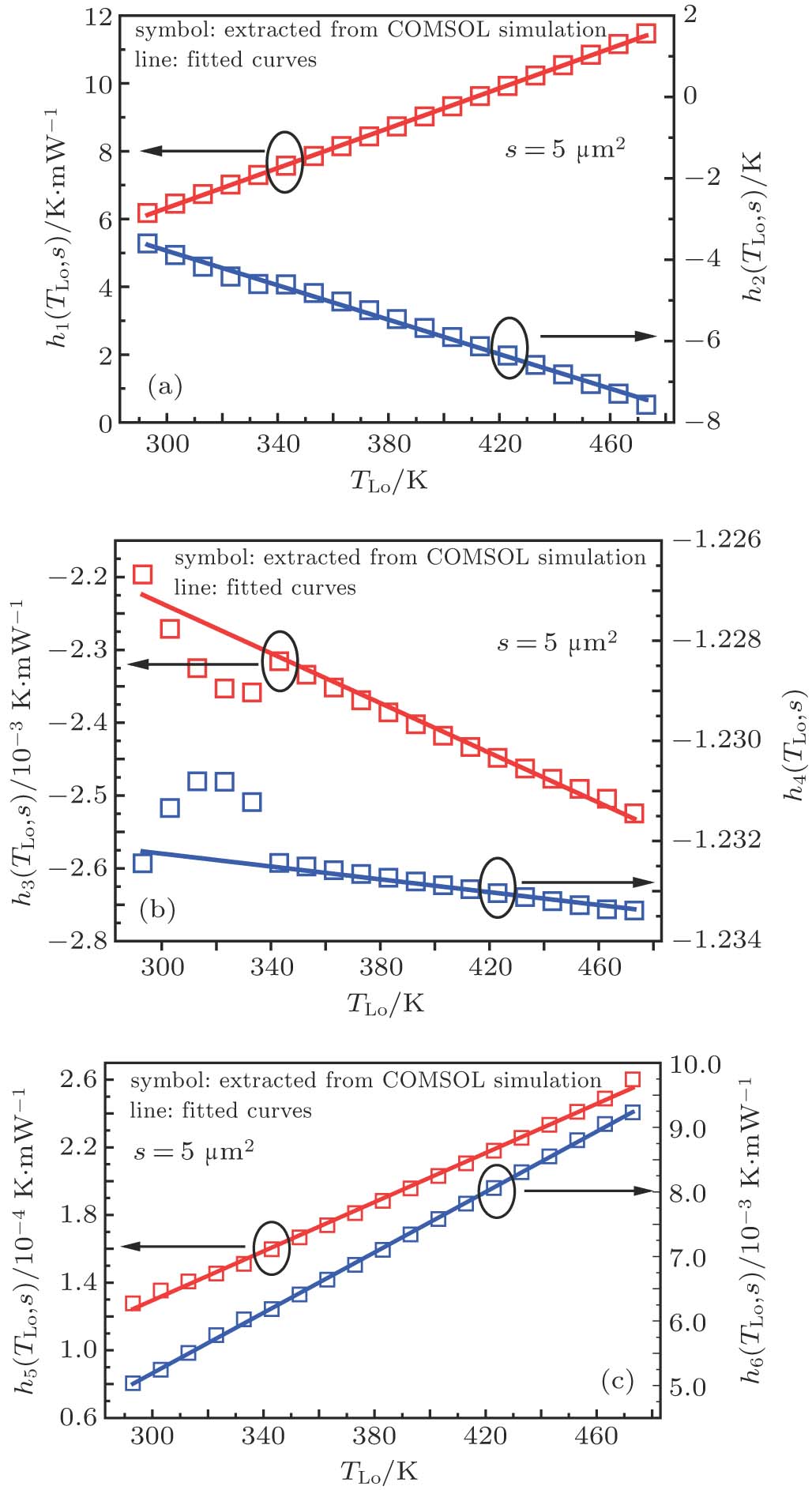
As shown in Fig. 10, are linearly related with TLo separately for the device with the emitter area of at 293 K, which can be expressed as follows:

Fig. 10. (color online) Relationships of with TLo.

Then, the functions of are fitted with s for four devices. Finally, the temperatures and expressed by Eqs. (1) and (7) are determined respectively. Furthermore, the obtained functions can also be re-used for the circuits with the same technology.

2.2. Temperature distribution for full IC chip

For an IC chip with n heat sources, the temperature increment at the center of heat source i is obtained by summing the temperature increment caused by source i itself and coupling heat from the sources of based on the principle of superposition.[32] Then the final junction temperature at the center of heat source i can be written as

where Ta is the initial ambient temperature, is its own temperature increment, is the temperature increment based on the thermal coupling effect from other devices, and is the temperature increment from the coupled heat source k. Therefore, the new equivalent local temperature can be calculated from Eq. (6).

Based on Eq. (6) and the calculation steps, such as Steps 1.1 to 1.2 or Steps 2.1 to 2.4, the junction temperature T of each device can be worked out sequentially by SATSM or SATSM-I to obtain the temperature distribution of the circuit. Also, this method can be generally applied to the thermal analysis for various kinds of semiconductor integrated circuits as long as the geometric models are applied to the corresponding devices in COMSOL.

3. Thermal analysis for compound semiconductor integrated circuits

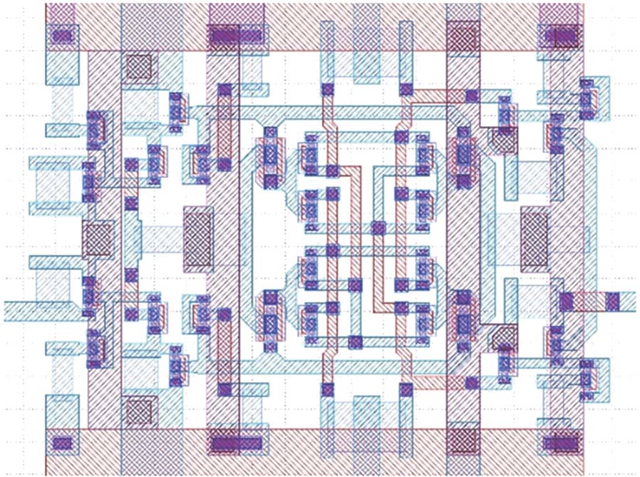
In this section, the method will be applied to the actual circuits. The SATSM and SATSM-I are codified by MATLAB on a Lenovo QiTianM6500-N000 desktop computer with 8-GB memory and an Intel(R) CoreTM i5-4570 CPU @3.20 GHz. The COMSOL is operated on a DELL R730 server with 128-GB memory and 2 Xeon (R) E–2683 V3 CPUs @2.00 GHz. The first example is an InP HBT frequency divider, which is a small scale IC. The layout of the circuit is shown in Fig. 11, in which 28 transistors are included.

Fig. 11. (color online) Layout of InP HBT frequency divider.

The initial ambient temperature and local temperature surrounding the individual device are set to be 300 K. The calculations of the center temperature for each of all the devices are accomplished within 0.54 second and 0.69 second by SATSM and SATSM-I respectively, and the thermal profiles of the devices in the frequency divider are mapped using MATLAB for 28 devices and shown in Fig. 12(a). It is obvious that the farther the distance from the center of the device, the lower the temperature is. The maximum temperature is 361.03 K located in the center position of the device of No. 13, owing to its higher dissipated power.

Fig. 12. (color online) Thermal profiles of frequency divider, obtained from (a) SATSM-I and (b) COMSOL.

In order to validate the temperature distribution, the simulation of the temperature distribution is performed by using COMSOL with a great number of grids, costing CPU time of about 3 hours with the peak memory usage of 100 GB as shown in Fig. 12(b). Therefore, it can be concluded that SATSM and SATSM-I are more efficient than COMSOL. Comparing Fig. 12(a) with Fig. 12(b), the maps of the two thermal profiles are consistent with each other. However, there are differences between these two thermal profiles of the full circuit somewhat, because the number of the meshes in COMSOL is far more than that in SATSM-I.

Table 2 shows the junction temperatures of the devices obtained by using the COMSOL, SATSM, and SATSM-I. Due to the longitudinal symmetry of layout, there are only 14 devices listed in Table 2 and their locations are shown in Fig. 12(a). It can be obviously seen that the results from SATSM-I match the results from COMSOL very well. Furthermore, the mean relative error of the SATSM-I is reduced by 19.35%, which decreases significantly compared with that of SATSM.

Table 2.

Comparison among temperatures of frequency divider, obtained from SATSM, SATSM-I, and COMSOL.

.

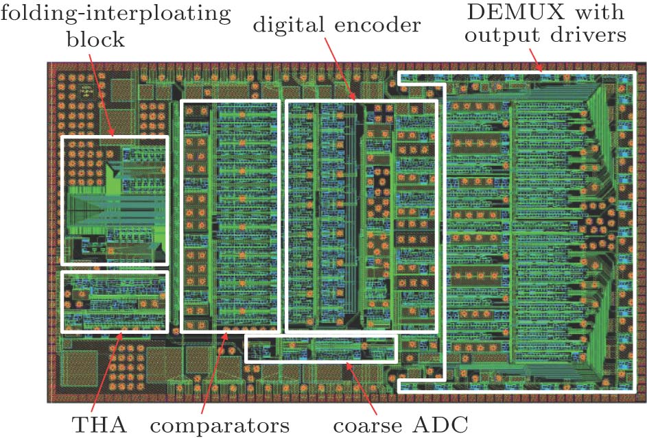
In order to verify the proposed method for large scale IC, a 6-bit 3-Gsps ADC chip is used as a testing example, including 3449 GaAs HBTs processed with GaAs HBT technology. Figure 13 shows the full layout of the ADC chip, which consists of THA, folding-interpolating block, digital encoder, etc.

Fig. 13. (color online) Full layout of GaAs HBT ADC chip.

For more than 3 thousand devices, a huge quantity of calculations would take unbearable computation time and memory if the simulation is implemented by using the simulator COMSOL, leading to it being far beyond the capability of the computer. However, this problem can be easily solved by the proposed method with only 58.61 seconds and 242.70 seconds by SATSM and SATSM-I respectively.

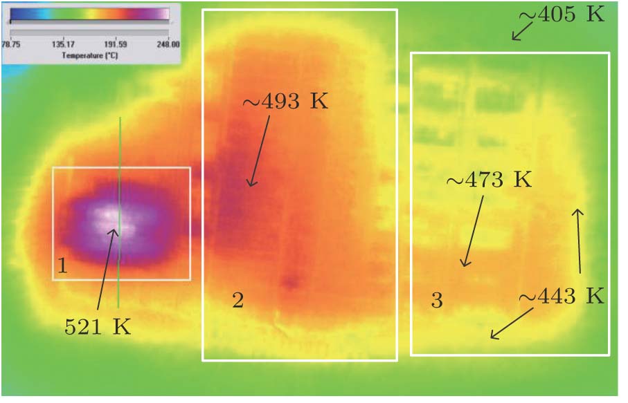
Figure 14 shows the temperature distribution and the isothermal distribution obtained from SATSM-I. In order to figure out the validity of the results from SATSM-I, the temperature distribution of the ADC chip is measured by an infrared thermal imager, and the thermal image of the ADC chip is shown in Fig. 15. As can be seen from Fig. 14(a), the temperatures of regions 1 and 2 are much higher than those of other parts of circuits because of their larger power dissipation. The highest temperature has reached 506 K located in region 1.
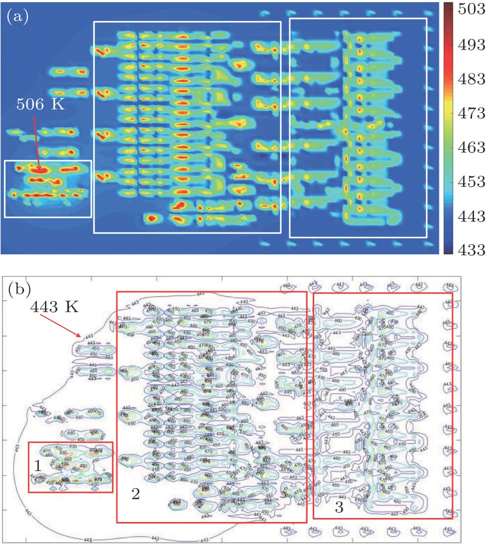
Fig. 14. (color online) (a) Temperature distribution and (b) isothermal distribution of ADC from SATSM-I.
Fig. 15. (color online) Thermal image of ADC chip.

From Fig. 14(b), it is clear to see that the temperature around the chip is about 443 K. Owing to the lower resolution, the thermal imager can only provide an average temperature in the related range, resulting in a little difference in temperature distribution between Fig. 14(a) and Fig. 15. It is found from Fig. 15 that the ambient temperature of the chip is about 405 K from the green area outside the chip, and the yellow part around the chip is 443 K approximately. The purple and white parts in region 1 are the high-temperature area, with a maximum temperature of about 521 K.

Table 3 shows the results of the chip temperatures, calculated by SATSM-I and SATSM, and also the temperature measured by the infrared thermal imager. Comparing with the measured values, the difference in the highest temperature is 15 K with a relative error of 2.88% obtained by SATSM-I. The SATSM-I reduces the error by 55.56%, compared with the results calculated by the SATSM. For the lower dissipated power than the THA circuit in region 1, the highest temperatures in regions 2 and 3 and the temperature around the chip calculated by SATSM-I are about 493 K and 473 K, which are the same as the measured values, because the variation of thermal conductivity is taken into consideration in implementing the temperature superposition by iterative algorithm.

Table 3.

Comparisons between chip temperatures calculated by SATSM-I and SATSM with measured values

.

As shown from Table 3, the accuracy of SATSM-I is improved more than that of SATSM. However, the temperatures calculated by SATSM-I are almost the same as the measured values except in the highest temperature region, for which the most important reason is that the power dissipation of each device used in the calculation is obtained in circuit simulation software with constant local temperature. Actually, the power dissipation for each device increases with the increase of local temperature in operation because of the temperature positive feedback. Therefore, the difference between the actual temperature and the calculated temperature by SATSM-I or SATSM must be more obvious in the high temperature region. Due to the fact that the thermal radiation of the chip is affected by the surface layer material and the air, the temperature of the thermal image is lower than the actual temperature inside the chip. Therefore, the temperatures calculated by SATSM-I are very close to those from the thermal image. In addition, the interconnections and vias are not considered in the simplified model, which can induce a certain error in calculation. In the proposed method, it is difficult to address all the relevant effects in a single study and therefore further research is needed to strengthen the model. Nevertheless, the modeled results agree well with the measured temperature distribution of the full chip, which demonstrates that the SATSM-I proposed in this paper is effective and suitable for predicting the temperature of a large scale IC with high accuracy and high efficiency.

4. Conclusions

In summary, an efficient thermal analysis method SATSM-I has been presented for large scale compound semiconductor ICs based on HBT. Considering the temperature dependence of thermal conductivity on the thermal coupling effect and self-heat effect, the accuracy of the calculated result from the SATSM-I is significantly improved compared with the SATSM dealing with a fixed thermal conductivity, especially for the higher temperature region. However, the SATSM is also a good choice if power dissipation is lower because of its high efficiency and simplicity of calculation. Moreover, a relative error of the highest temperature from SATSM-I is only about 2.88%, achieving high efficiency operation. It is demonstrated that the proposed SATSM-I can be used in the calculation of temperature distribution and the thermal analysis design for a large scale compound semiconductor IC. Also, this method would be easily applied to other kinds of large scale integrated circuits.

Reference
[1] Hossain M Nosaeva K Janke B Weimann N Krozer V Heinrich W 2016 IEEE Microw. Wirel. Compon. Lett. 26 23
[2] Li O P Zhang Y Xu R M Cheng W Wang Y Niu B Lu H Y 2016 Chin. Phys. 25 058401
[3] Yamamoto K Miyashita M Maki S Takahashi Y Fujii K Fujiwara S Kitabayashi F Suzuki S Shimura T Hieda M Seki H 2016 IEEE Trans. Microw Theory. Tech. 64 810
[4] Kang S Kim D Urteaga M Seo M 2017 Proc. IEEE Int. Symp. Radio-Freq. Integr. Technol. (RFIT) August 30–Septemper 1, 2017 Seoul, South Korea 25 10.1109/rfit.2017.8048278
[5] Ge J Liu H G Su Y B Cao Y X Jin Z 2012 Chin. Phys. 21 058501
[6] Luong M D Ishikawa R Takayama Y Honjo K 2017 IEEE Trans. Circuits Syst. I Reg. Papers 64 1140
[7] Coquillat D Nodjiadjim V Blin S Konczykowska A Dyakonova N Consejo C Nouvel P Pènarier A Torres J But D Ruffenach S Teppe F Riet M Muraviev A Gutin A Shur M Knap W 2016 Int. J. High Speed Electron Syst. 25 164001
[8] Urteaga M Griffith Z Seo M Hacker J Rodwell M J W 2017 Proc. IEEE 105 1051
[9] Lin L Zhou L Wang R Tong L Yin W Y 2015 IEEE Trans. Microw Theory. Tech. 63 1951
[10] Kim J Jeon S Kim M Urteaga M Jeong J 2015 IEEE Trans. Terahertz. Sci. Technol. 5 215
[11] Baek S Ahn H Nam I Ryu N Lee H D Park B Lee O 2016 IEEE Microw Wirel. Compon. Lett. 26 921
[12] Grandchamp B Nodjiadjim V Zaknoune M Koné G A Hainaut C Godin J Riet M Zimmer T Maneux C 2011 IEEE Trans. Electron Devices. 58 2566
[13] Su J L Tseng H C 2017 IEEE Trans. Device Mater. Rel. 17 678
[14] Sukwon S Peake G M Keeler G A Geib K M Briggs R D Beechem T E Shaffer R A Clevenger J Patrizi G A Klem J F Tauke-Pedretti A Nordquist C D 2016 IEEE Trans. Compon. Packag. Manuf. Technol. 6 740
[15] Koné G A Grandchamp B Hainaut C Marc F Maneux C Labat N Zimmer T Nodjiadjim V Riet M Godinb J 2011 Microelectron. Reliab. 9 1730
[16] Kone G A Maneux C Labat N Zimmer T Grandchamp B Frijlink P Maher H 2012 Int. Conf. Indium Phosphide Relat. Mater. August 27–30, 2012 Santa Barbara, USA 208 10.1109/iciprm.2012.6403359
[17] Tao N Lin B Lee C Henderson T Lin B 2015 Int. J. Microw. Wirel. Technol. 7 279
[18] Chivukula V Teeter D Scott P Shah B Ji M 2014 Microelectron. Reliab. 54 2688
[19] Liu X Yuan J Liou J 2011 Microelectron. Reliab. 51 2147
[20] Ozalas M T 2014 Proc. Compound Semicond. Integr. Circuit Symp. (CSIC) October 19–22, 2014 La Jolla, USA 1 10.1109/csics.2014.6978582
[21] Li P Pileggi L T Asheghi M Chandra R 2006 IEEE Trans. Comput-Aided Design Integr. Circuits Syst. 25 1763
[22] Yu W Zhang T Yuan X Qian H 2013 IEEE Trans. Comput-Aided Design Integr. Circuits Syst. 32 2014
[23] Feng Z Li P 2013 IEEE Trans. Very Large Scale Integr. (VLSI) Syst. 21 1526
[24] Liu S S Y Luo R G Aroonsantidecha S Chin C Y Chen H M 2014 IEEE Trans. Very Large Scale Integr. (VLSI) Syst. 22 1404
[25] Zhang C Han Q G Ma H A Xiao H Y Li R Li Z C Tian Y Jia X P 2010 Acta Phys. Sin. 59 1923 (in Chinese) http://wulixb.iphy.ac.cn/CN/Y2010/V59/I3/1923
[26] Zheng Y B Yao J Q Zhang L Wang Y Wen W Q Jing L Di Z G 2012 Chin. Phys. Lett. 29 024203
[27] Grasser T Selberherr S 2000 Proc. Int. Semicond. Conf. October 10–14, 2000 Sinaia, Romania 43 10.1109/smicnd.2000.890187
[28] Zhang J C Zhang Y M Lu H L Zhang Y M Xiao G H Ye G P 2014 J. Semicond. 35 08005
[29] Palankovski V 2000 Simulation of heterojunction bipolar transistors Ph. D. Dissertation Vienna Vienna University of Technology
[30] Harrison I Dahlstrom M Krishnan S Griffith Z Kim Y M Rodwell M J W 2004 IEEE Trans. Electron Dev. 51 529
[31] Matsuda T Hanai H Tohjo T Iwata H Kondo D Hatakeyama T Ishizuka M Ohzone T 2014 IEEE Trans. Semicond. Manuf. 27 151
[32] Cheng Y K Kang S M 2000 IEEE Trans. Comput-Aided Design Integr. Circuits Syst. 19 1211