Transport spectroscopy through dopant atom array in silicon junctionless nanowire transistors
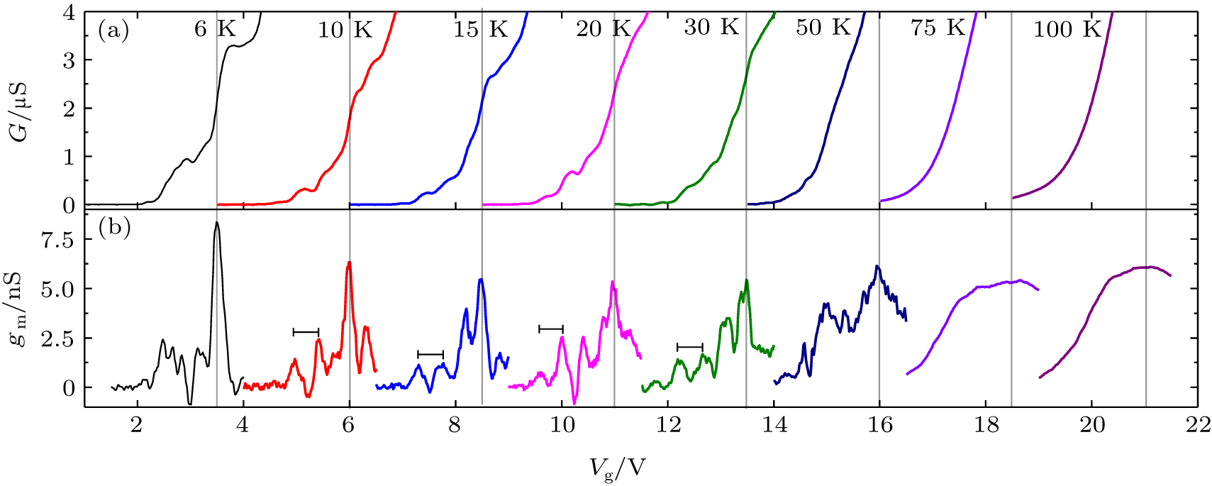
(color online) (a) Conductance curves G–Vg (a) and (b) transconductance curves gm–Vg at Vds = 10 mV for different temperatures. The curves at each temperature are systematically shifted for the clarity of the fine current steps. The values of gate voltage spacing of two transconductance peaks are 0.464 V at 10 K, 15 K, 30 K and 0.4 V at 20 K, respectively.