Transport spectroscopy through dopant atom array in silicon junctionless nanowire transistors
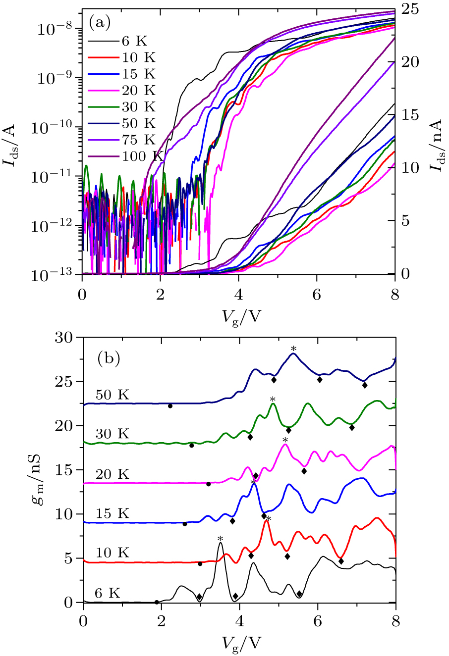
(color online) (a) Drain current Ids and (b) transconductance gm (gm = ∂Ids/∂Vgs) versus gate voltage Vg of a single channel JNT at Vds = 10 mV at different temperatures. The curves in panel (b) are shifted for clarity.