Transport spectroscopy through dopant atom array in silicon junctionless nanowire transistors
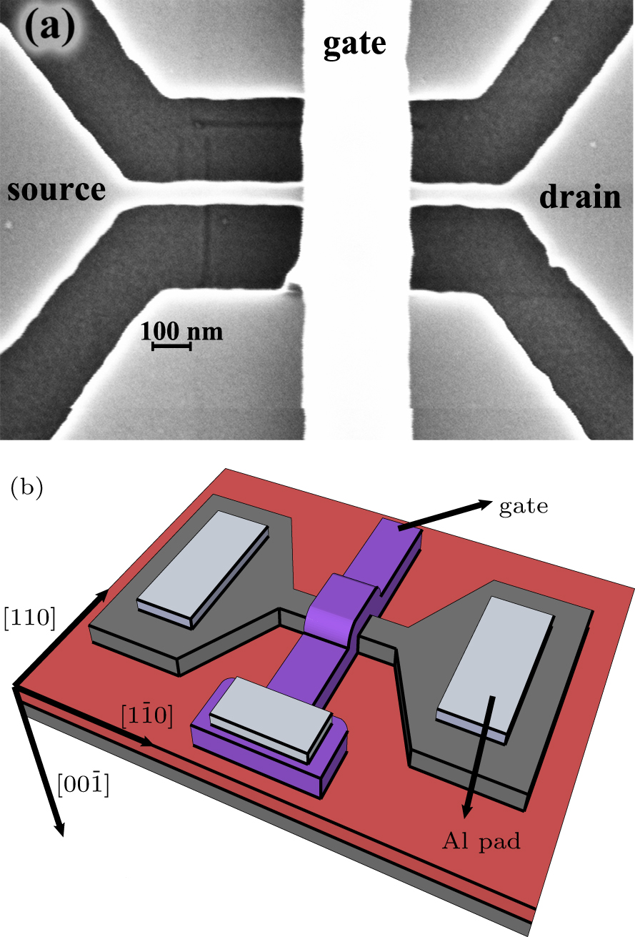
(color online) (a) Top view SEM image of our device after gate formation. The cross section of channel is 18 nm × 30 nm and the gate length is 280 nm. (b) Three-dimensional schematic of JNT after Al pad formation.