Visualizing light-to-electricity conversion process in InGaN/GaN multi-quantum wells with a p–n junction
Project supported by the National Key Research and Development Program of China (Grant Nos. 2016YFB0400302 and 2016YFB0400603), the National Natural Science Foundation of China (Grant Nos. 11574362, 61210014, and 11374340), and the Innovative Clean-Energy Research and Application Program of Beijing Municipal Science and Technology Commission, China (Grant No. Z151100003515001).
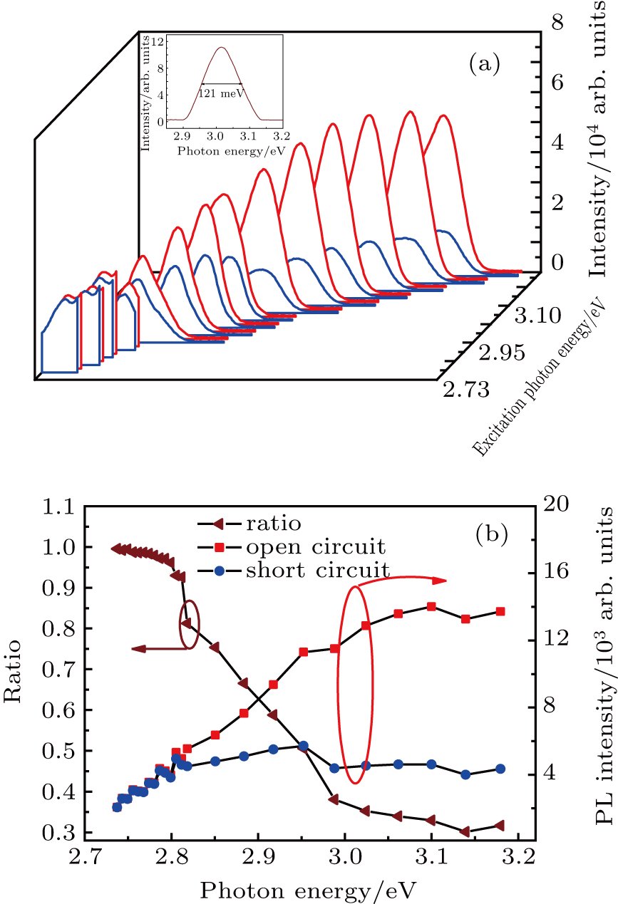
(color online) (a) PL spectra excited at changing excitation photon energy from 3.18 eV to 2.75 eV. The red and blue curves represent the PL intensities under open and short circuit conditions, respectively. The inset shows the line width of the incident beam due to the sample scattering and limit of the resolution of the monochromator, which is about 121 meV when the incident photon energy is 3.02 eV. (b) The excitation wavelength dependent PL integrated intensities and the ratio of the PL integrated intensity under open circuit condition to short circuit condition.
