Project supported by the National Natural Science Foundation of China (Grant Nos. 51290271 and 11474364), the National Basic Research Program of China (Grant Nos. 2013CB933601 and 2013YQ12034506), the Natural Science Funds for Distinguished Young Scholars of Guangdong Province, China (Grant No. 2014A030306017), the Pearl River S & T Nova Program of Guangzhou, China (Grant No. 201610010084), and the Guangdong Special Support Program, China.
Project supported by the National Natural Science Foundation of China (Grant Nos. 51290271 and 11474364), the National Basic Research Program of China (Grant Nos. 2013CB933601 and 2013YQ12034506), the Natural Science Funds for Distinguished Young Scholars of Guangdong Province, China (Grant No. 2014A030306017), the Pearl River S & T Nova Program of Guangzhou, China (Grant No. 201610010084), and the Guangdong Special Support Program, China.
† Corresponding author. E-mail:
Project supported by the National Natural Science Foundation of China (Grant Nos. 51290271 and 11474364), the National Basic Research Program of China (Grant Nos. 2013CB933601 and 2013YQ12034506), the Natural Science Funds for Distinguished Young Scholars of Guangdong Province, China (Grant No. 2014A030306017), the Pearl River S & T Nova Program of Guangzhou, China (Grant No. 201610010084), and the Guangdong Special Support Program, China.
All-solid-state strong coupling systems with large vacuum Rabi splitting energy have great potential applications in future quantum information technologies, such as quantum manipulations, quantum information storage and processing, and ultrafast optical switches. Monolayer transition metal dichalcogenides (TMDs) have recently been explored as excellent candidates for the observation of solid-state strong coupling phenomena. In this work, from both experimental and theoretical aspects, we explored the strong coupling effect by integrating an individual plasmonic gold nanorod into the monolayer tungsten diselenide (WSe2). Evident anti-crossing behavior was observed from the coupled energy diagram at room temperature; a Rabi splitting energy of 98 meV was extracted.
By integrating a specific quantum emitter into an optical cavity, its optical response can be modified substantially owing to the variation in the local electromagnetic environment within the cavity. In particular, if the interaction between the emitter and optical cavity is sufficiently strong to overwhelm their respective dissipation rates, a strong coupling regime is achieved.[1,2] In this regime, hybridized energy states with part-light and part-matter characteristics are formed, which can be observed from the optical spectra of the system as mode splitting, or, in a quantum mechanics language, the Rabi splitting (RS). The strong coupling effects can form the basis of many quantum optics applications, such as quantum manipulation, quantum information storage and processing, and ultrafast single-photon switches.[3–5] Consequently, several systems with a strong coupling effect have been proposed and systematically studied, including atoms placed in optical microcavities,[6] quantum dots integrated with photonic crystals,[2,7] quantum wells embedded into distributed Bragg reflectors (DBR) cavities,[8] and organic molecules coupled with plasmonic nanocavities.[9–11]
From an application point of view, an all-solid-state system operating at room temperature and having easily accessible large RS is preferred. Whereas the aforementioned systems are demonstrated with robust and evident strong coupling effects, they are either non-solid-state or suffering from complex operation conditions, such as ultrahigh vacuum and cryogenic temperature. Theoretically, the coupling strength g, which is equal to half of the RS, is determined by
 |

In recent years, two-dimensional transition-metal dichalcogenides (TMDs) have attracted significant attention because of their excellent optical and optoelectronic responses associated with their two-dimensional exciton transitions.[13–18] Monolayer TMDs usually exhibit large exciton binding energies of 0.3–0.9 eV, which is much larger than the thermal activation energy at room temperature (25 meV). In addition, the overlap of the electron–hole wave functions in two-dimensional plane of the monolayer TMDs is very strong because of their atomic thicknesses, which enhances transition dipole moments of the two-dimensional excitons.[19] On the other hand, TMDs can also endow the strong coupling effects with intriguing functionalities that are derived from their specific excitonic characteristics, such as tenability and valley-controlled optical response, which can open up new avenues for both fundamental research and practical applications.[20] Eventually, several studies have demonstrated the strong coupling effects by integrating TMDs with various optical micro- and nanocavities.[21–25]
Recently, we have realized an all-solid-state system exhibiting room-temperature Rabi splitting with active control in a heterostructure consisting of monolayer WS2 and an individual plasmonic gold nanorod.[26] By taking advantage of the large transition dipole moment of the WS2 exciton, giant Rabi splitting energies of ∼ 133 meV can be achieved at ambient conditions. Practical optoelectronic applications usually require building blocks with multiple functionalities that are derived from different materials. Hence, we generalized the strong coupling studies of TMDs to heterostructures composed of an individual Au nanorod and monolayer WSe2. In comparison with WS2, the monolayer WSe2 exhibits a smaller bandgap and a 10 times higher electron mobility, which has great application potential in infrared optoelectronic devices. We show that the dipolar plasmon resonance of gold nanorod can lead to strong localized electromagnetic fields on the surface of the WSe2, giving rise to coherent interaction between the two-dimensional excitons and plasmon resonance. Evident anti-crossing behavior can be observed from the coupled energy diagram of the heterostructures, whereby an RS up to 98 meV is extracted. One should note that a recent study has demonstrated the strong coupling effect by integrating the monolayer WSe2 with an individual silver nanowire, where high-order Fabry-Pérot cavity mode of the nanowire was employed.[27] In our study, the dipolar plasmon resonance mode was utilized, which resulted in a two-times higher RS energy in comparison with the previous study.
Gold nanorods were grown using a seed-mediated method.[28] Briefly, the seed solution was prepared by adding a freshly prepared ice-cold NaBH4 aqueous solution (0.6 mL, 0.1 M) into a mixture solution composed of HAuCl4 solution (0.25 mL, 0.01 M) and CTAB solution (9.75 mL, 0.1 M). Afterwards, rapid inversion-mixing was performed for 2 min. The seed solution was kept at room temperature for 2–6 h before use. The growth solution was made by sequential addition of HAuCl4 (2.0 mL, 0.01 M), AgNO3 (0.4 mL, 0.01 M), HCl (0.16 mL, 5 M), and AA (0.32 mL, 0.1 M) to the CTAB solution (40.0 mL, 0.1 M). The gold nanorods were obtained by adding the seed solution (20 μL) into the growth solution. The resulting mixture was left undisturbed at room temperature overnight. The monolayer WSe2 flake was grown by the chemical vapor deposition (CVD) method. To prepare the heterostructure, the gold nanorods were deposited onto the monolayer WSe2 flake by drop-casting. Various heterostructures can be obtained after the droplet dried naturally under ambient conditions.
The scattering spectra of individual gold nanorods–WSe2 heterostructure were recorded on a dark-field optical microscope (Olympus BX51) that was integrated with a quartz-tungsten-halogen lamp (100 W), monochromator (Acton SpectraPro 2360), and charge-coupled device camera (Princeton Instruments Pixis 400BR_eXcelon). The camera was thermoelectrically cooled to −70 °C during the measurements. A dark-field objective (100×, numerical aperture 0.80) was employed for both illuminating the heterostructures with the white excitation light and collecting the scattered light.
The extinction spectra of the gold nanorods aqueous solution were measured on a HITACHIU-4100 UV/visible/near-infrared spectrophotometer. The Raman and photoluminescence (PL) spectra of the monolayer WSe2 were collected using a Renishaw inVia Reflex system integrated with a dark-field microscope (Leica). The 532-nm excitation laser was focused onto the samples with a diameter of ∼ 1 μm through a 50× objective (NA = 0.8).
SEM images of individual heterostructures were acquired using an FEI Quanta 450 microscope. The thickness of the monolayer WSe2 was measured using an atomic force microscope (AFM, NTEGRA Spectra). High-resolution transmission electron microscopy (HRTEM) and selected-area electron diffraction measurements were conducted on the same TEM system (FEI Tecnai3 G2 60-300), with an operation voltage of 300 kV.
The FDTD method was utilized to calculate the optical properties of the various heterostructures. The individual gold nanorod was modeled as a cylinder capped with hemispheres at each end that was placed on a WSe2 layer on top of a 300-nm-thick SiO2 layer. The bulk dielectric function of gold was used for the calculations.[29] The dielectric function of the monolayer WSe2 was adopted from previously reported values.[30] In this manner, the exciton energy was determined to be 1.66 eV. A dielectric constant of 2.25 was used for the SiO2 substrate. For the calculation of scattering spectra of the heterostructures, the lengths and diameters of gold nanorods were set to (78 nm, 26 nm), (80 nm, 25 nm), (81 nm, 24 nm), (83 nm, 24 nm), (86 nm, 24 nm), and (87 nm, 20 nm). The thickness of the WSe2 monolayer was set to 1 nm.
The strong coupling effect can be phenomenologically described using a coupled harmonic oscillator model,[10,25]
 |
 |

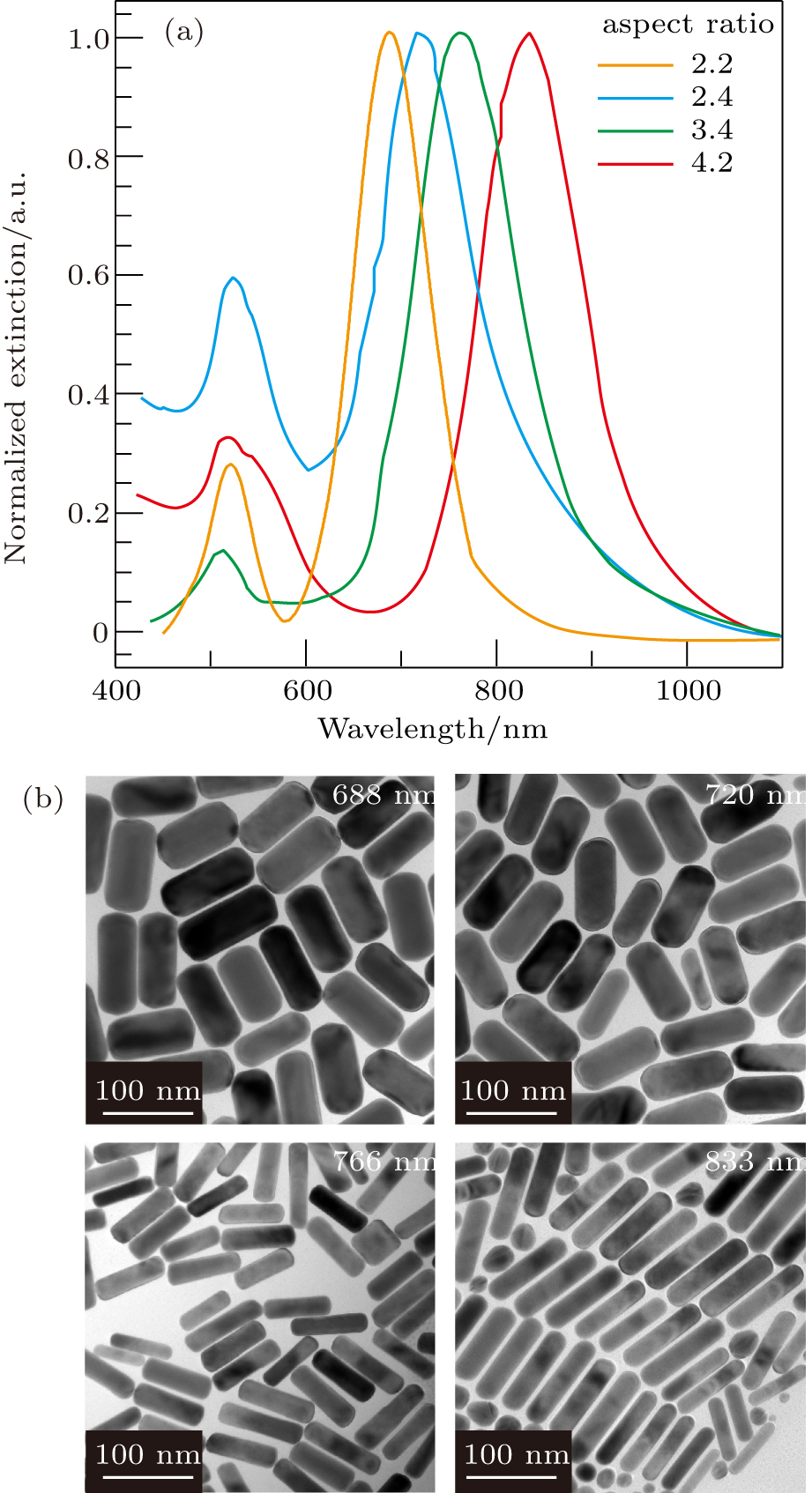
Usually, the elongated gold nanorods exhibit two types of dipolar plasmon resonances: one is the transverse plasmon mode (TPM) associated with electron oscillations along the diameter direction, and the other is the longitudinal one (LPM) originated from the electron oscillations along the length direction.[31] The operation wavelength of the TPM is usually located at ∼ 530 nm irrespective of the aspect ratio of the nanorod. In contrast, the LPMs exhibit wavelengths that are nearly linearly dependent on the aspect ratio of the nanorod.[28] Such a characteristic makes the gold nanorod an excellent nanocavity for studying the strong coupling behavior. By synthetically tuning the nanorod aspect ratio, different LPM wavelengths can be generated allowing us to scan across the fixed exciton transition energy; hence, regimes with varied coupling strengths can be obtained.
By increasing the aspect ratios of the nanorod samples, the LPM wavelengths can be progressively redshifted from 688 nm to 833 nm (Fig.
The WSe2 sample used in our study had a triangular shape with an edge length of ∼ 50 μm (Fig. 
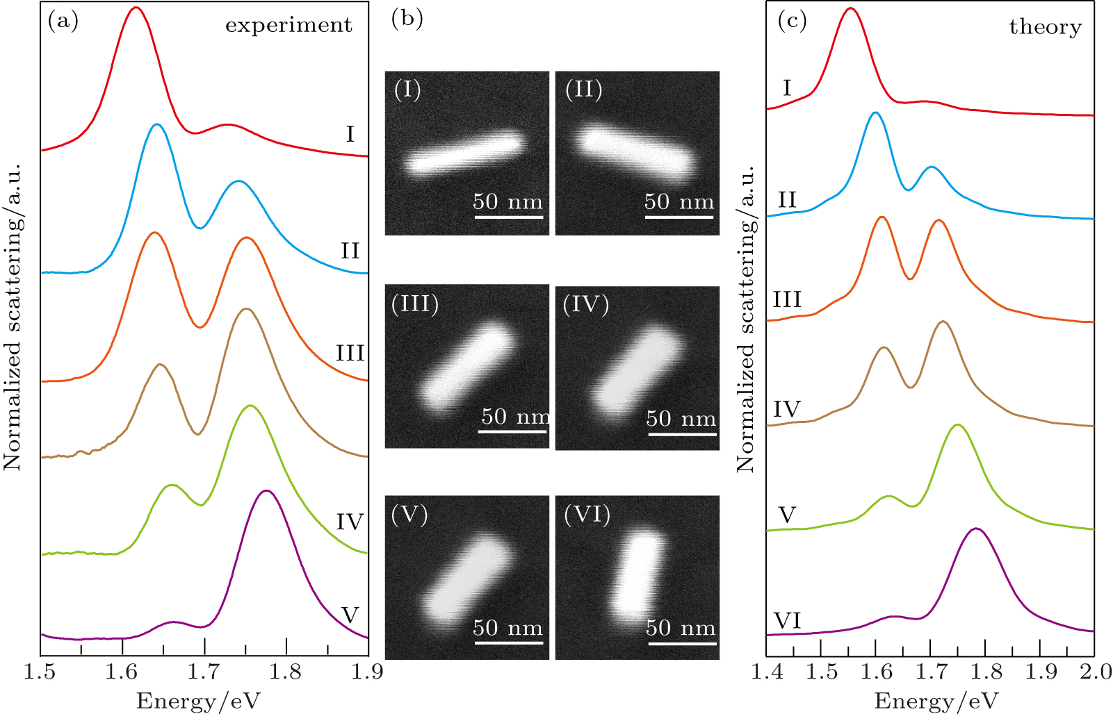
In our study, we employed single-particle dark-field scattering microscopy to study the strong coupling effect in an individual heterostructure; it allows us to get rid of extrinsic factors such as the inhomogeneous size distribution of plasmonic nanocrystals, background scattering, or aggregation of nanocrystals.[33,34] To that end, gold nanorods with different aspect ratios were dispersed onto the monolayer WSe2 flake to form various gold nanorod-WSe2 heterostructures, whereby a pattern-matching method was employed to correlate the geometry of each heterostructure and its scattering spectrum (Fig.
To thoroughly study the interaction between the LPM and excitons, scattering spectra from various gold nanorod-WSe2 heterostructures with different detunings between the plasmon and exciton transition energies were measured. The detunings were controlled by selecting heterostructures with specific gold nanorod aspect ratios. Figure
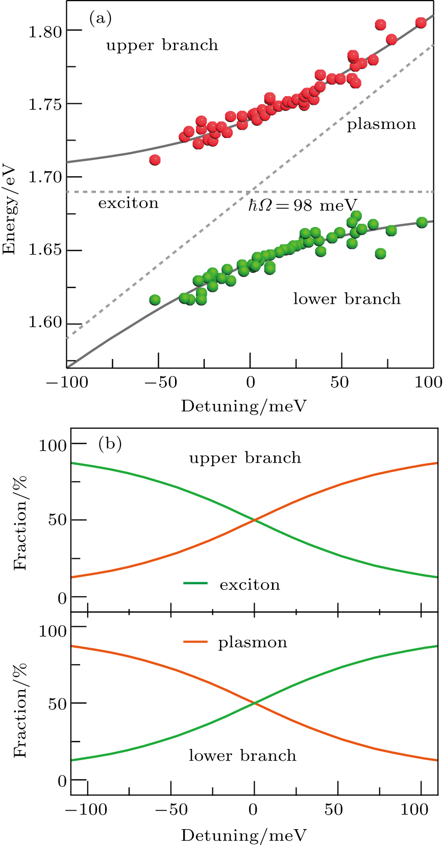
To further reveal the coupling regime of the heterostructures, the coupled energy diagram demonstrating the dependence of the two hybrid modes on the detunings was inspected. As shown in Fig.
 |
The strong coupling between the LPM resonance and exciton transition is mediated by the localized plasmonic field.[12,36] Namely, the nanorod acts as an antenna to focus the free-space electromagnetic field into the gap between the nanorod and WSe2. Such a localized field can thereafter excite the exciton transition of the WSe2. As a result, energy transfer between the plasmonic field and transition dipole moment can occur when the exciton is in its excited state. According to this coupling mechanism, the strong coupling should be rigorously dependent on the separation between the nanorod and WSe2. Figure
 | Fig. 6. Calculated scattering spectra of heterostructures with different separations between the gold nanorod and the WSe2 surface. The aspect ratio of the gold nanorod is kept as 3.5. |
The all-solid-state strong coupling system revealed in our study might have great potential in future quantum information technology, where long coherence time of the qubits is desired. However, in our current study the experimental configuration is very simple and only suitable for revealing the underlying beautiful physics. To make practical devices that are compatible with transmitting and processing information nowadays, one needs to expand the individual Au nanorod-WSe2 heterostructure into an array structure. In such a manner, the array structure can be excited by a laser beam that is focused down to the diffraction-limit scale as used in many nanophotonic devices. In addition, the optical response of the array can be collected and characterized by ordinary reflection and transmission microscopy, which are more compatible with optical systems nowadays.
In summary, we have revealed the strong coupling effect between the LPM resonance of an individual gold nanorod and two-dimensional exciton in monolayer WSe2 flake. By employing single-particle dark-field scattering spectroscopy, strong coupling with evident RS was observed from the scattering spectra of the gold nanorod-WSe2 heterostructures. In addition, anti-crossing behavior was revealed from the coupled energy diagram by changing the energy detunings between the LPM resonance and exciton transition, where an RS energy of 98 meV was extracted. We believe that the proposed gold nanorod-WSe2 heterostructures can pave the way for exploring the strong coupling of all-solid-state systems in the near-infrared regime, which has a potential for application in future quantum optics and quantum information processing technologies.
| [1] | |
| [2] | |
| [3] | |
| [4] | |
| [5] | |
| [6] | |
| [7] | |
| [8] | |
| [9] | |
| [10] | |
| [11] | |
| [12] | |
| [13] | |
| [14] | |
| [15] | |
| [16] | |
| [17] | |
| [18] | |
| [19] | |
| [20] | |
| [21] | |
| [22] | |
| [23] | |
| [24] | |
| [25] | |
| [26] | |
| [27] | |
| [28] | |
| [29] | |
| [30] | |
| [31] | |
| [32] | |
| [33] | |
| [34] | |
| [35] | |
| [36] |


