Intrinsic charge transport behaviors in graphene-black phosphorus van der Waals heterojunction devices
Project supported by the National Basic Research Program of China (Grant No. 2013CBA01600), the National Key Research & Development Project of China (Grant No. 2016YFA0202300), the National Natural Science Foundation of China (Grant Nos. 61474141, 61674170, 61335006, 61390501, 51325204, and 51210003), Youth Innovation Promotion Association of Chinese Academy of Sciences (Grant No. 20150005), and the China Postdoctoral Science Foundation (Grant No. 2017M623146).
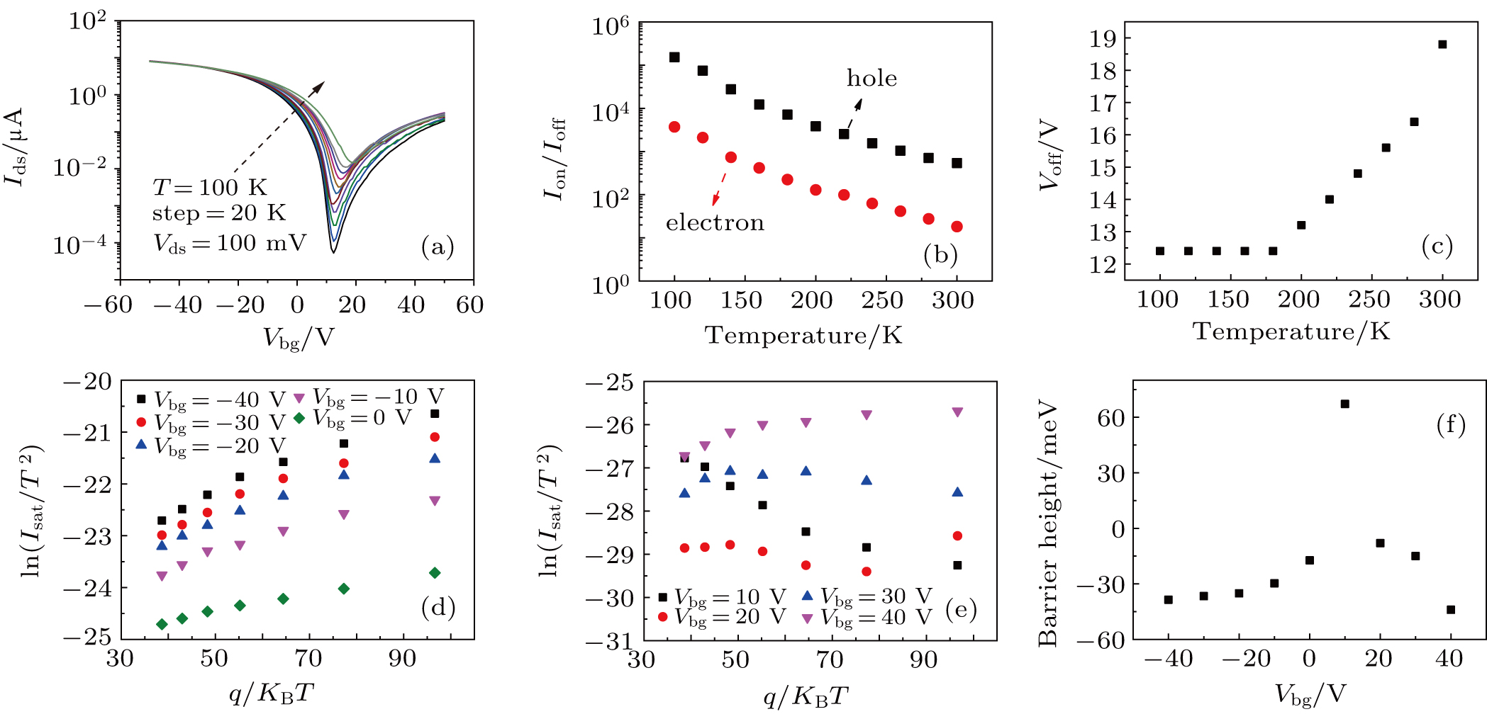
(color online) (a) Transfer curves of the heterojunction device at different temperatures from 100 K to 300 K at a step of 20 K under a constant bias voltage