Intrinsic charge transport behaviors in graphene-black phosphorus van der Waals heterojunction devices
Project supported by the National Basic Research Program of China (Grant No. 2013CBA01600), the National Key Research & Development Project of China (Grant No. 2016YFA0202300), the National Natural Science Foundation of China (Grant Nos. 61474141, 61674170, 61335006, 61390501, 51325204, and 51210003), Youth Innovation Promotion Association of Chinese Academy of Sciences (Grant No. 20150005), and the China Postdoctoral Science Foundation (Grant No. 2017M623146).
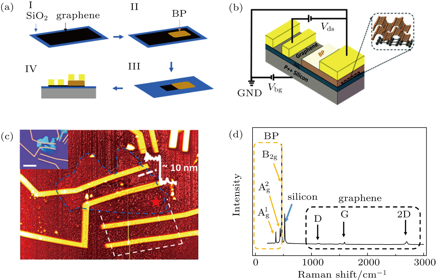
(color online ) (a) Schematic image of the device fabrication process. (b) Schematic image of the graphene/BP heterojunction device. (c) An AFM image of the heterojunction device. Section analysis shows the thickness of the BP flake is ∼ 10 nm. The inset is an optical microscope image of the device (scale bar inset is 10 μm). (d) Raman spectrum collected at the heterojunction region as indicated (red star) in (c).