Electronic properties of silicene in BN/silicene van der Waals heterostructures
Project supported by the National Key Research and Development Program of China (Grant No. 2016YFA0202300), the National Natural Science Foundation of China (Grant Nos. 61390501 and 61471337), the National Basic Research Program of China (Grant No. 2013CBA01600), the CAS Pioneer Hundred Talents Program, and the Beijing Nova Program, China (Grant No. Z181100006218023).
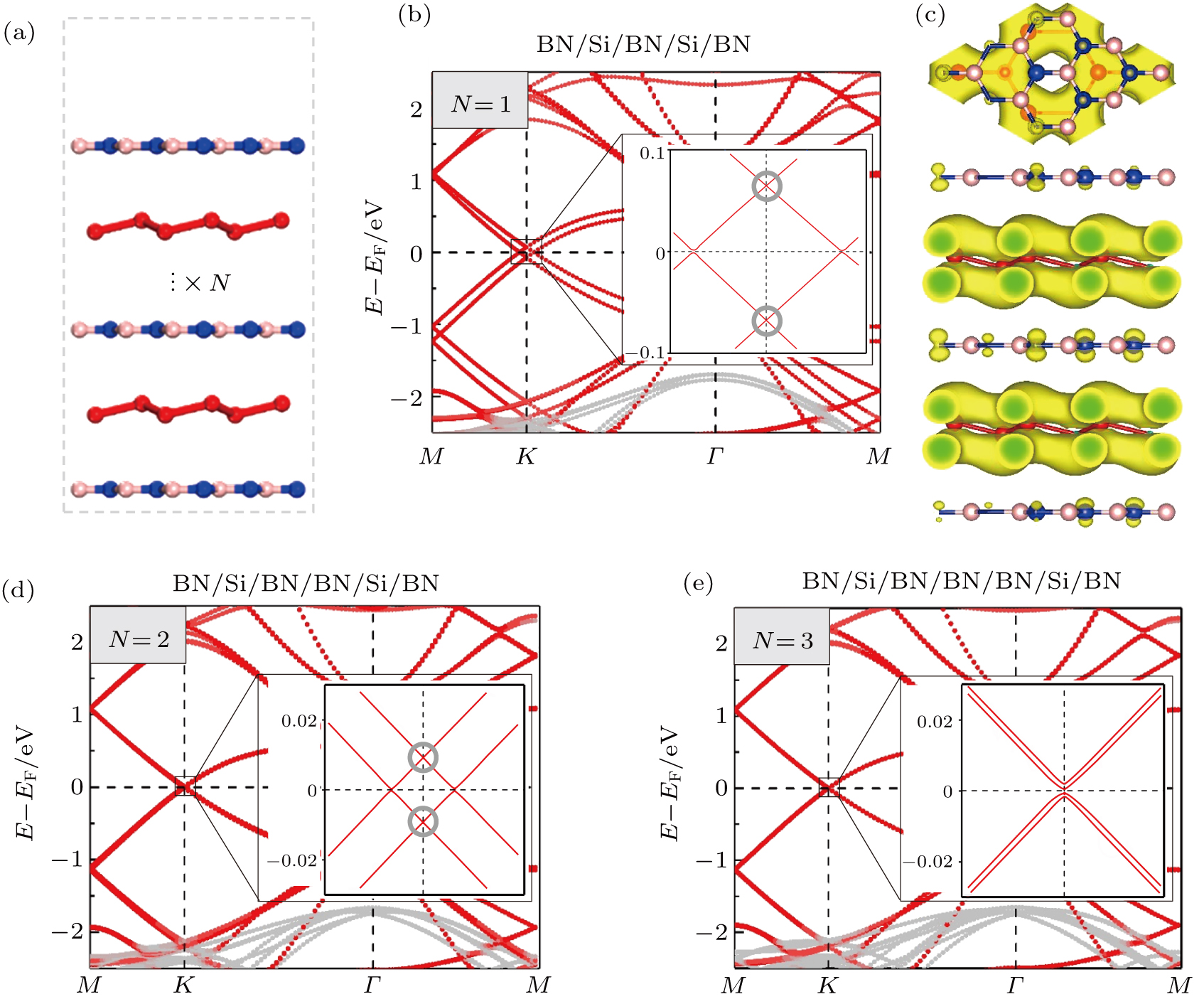
(color online) Coupling between silicene layers intercalated by BN layers. (a) Supercell of a 2D vdWHs with two silicene layers encapsulated inside but separated by
