Compact high-order quint-band superconducting band-pass filter*

Project supported by the National Natural Science Foundation of China (Grant Nos. 61371009 and 61401282) and the National Key Scientific Instrument and Equipment Development Project of China (Grant No. 2014YQ030975).

Wu Di1, Wei Bin1, †, Lu Xi-Long2, Lu Xin-Xiang3, Guo Xu-Bo1, Cao Bi-Song1
State Key Laboratory of Low-Dimensional Quantum Physics, Department of Physics, Tsinghua University, Beijing 100084, China
The No. 14 Research Institute, China Electronic Technology Corporation (CETC), Nanjing 210013, China
Department of Physics and Electronic Engineering, Shaoxing University, Shaoxing 312000, China


† Corresponding author. E-mail: weibin@mail.tsinghua.edu.cn

Project supported by the National Natural Science Foundation of China (Grant Nos. 61371009 and 61401282) and the National Key Scientific Instrument and Equipment Development Project of China (Grant No. 2014YQ030975).

Abstract

In this paper, we present a compact quint-band superconducting filter operating at 2.4, 3.5, 4.7, 5.3, and 5.9 GHz. Matching junctions with different impedance branch lines are used to connect a dual-band sub-filter with a tri-band sub-filter and to reduce the channel interactions. The quint-band filter design is divided into two sections to determine the controllable frequencies and bandwidths, while ensuring compact size and reducing design complexity. The filter is fabricated on double-sided YBCO film deposited on an MgO substrate with a size of 26 mm × 19 mm. The measured results match well with the simulations.

PACS: 85.25.-j
1. Introduction

Given the development of wireless communication systems, bandpass filters (BPFs) have aroused the increasing research interest of all.[13] Multi-band BPF is one of the most important front-end components. However, the addition of passband number leads to the increase of design difficulty and overall size. Few studies have reported quint-band BPFs or multi-band BPFs with more than five passbands.[47] In these studies, each BPF passband was generated by a single resonator or a pair of resonant modes, resulting in having only two or three poles on frequency response. Designing a high-order quint-band BPF with compact size, low insertion loss, and good selectivity is a great challenge.

Several methods of designing the multi-band BPFs have been developed and can be generally classified as three categories. The first category is to combine the BPFs, which have different resonant frequencies with common I/O ports. According to Ref. [8], the tri-band filter comprises three single-band sub-filters, in which each passband can be independently controlled. In a previous study,[9] two sets of resonators were employed to generate two dual-band responses, wherein these resonators are combined in parallel to achieve a quad-band filter. However, the overall size is large, especially for the designs with more than four passbands. The second category is to introduce the band-stop structures into a wideband BPF or transmission zeros (TZs) to a dual-band BPF to implement multi-band frequency responses.[10,11] This method has complicated design and fabrication with additional notch structures and is not suitable for widely spaced passbands. The third category is to use multi-mode resonators such as stepped-impedance resonators (SIRs),[1214] stub-loaded resonators (SLRs),[1517] and ring resonators.[1820] Nevertheless, high-order filters are hard to construct because the internal and external couplings of all passbands are difficult to adjust simultaneously.

High-temperature superconducting (HTS) thin films with extremely low microwave surface resistance can be used to produce multi-pole single passband filters with both low insertion and sharp rejection. A few attempts have been made at superconducting filters with four or more passbands. In Ref. [21], the author proposed a quad-mode stub-loaded resonator and quad-feeding structures to design high-order quad-band HTS filters. A quad-mode square ring loaded resonator is used to implement a second-order quad-band HTS filter in Ref. [22]. These researches indicated that using multi-mode resonators can hardly adjust the resonant mode and the coupling of each passband independently, and are difficult to extend to high-order quint-band HTS filters.

In the present paper, a new design method which combines two different multi-band sub-filters into a quint-band BPF is proposed. A compact high-order superconducting quint-band filter is also presented. The first two passbands are constructed by four stub-loaded stepped-impedance resonators (SL-SIRs). The resonant characteristics are investigated and the harmonic frequencies are pushed upwards to prevent them interfering with the rest of the passbands. Moreover, three different types of resonators are combined to form a tri-band response, which corresponds to the last three passbands. A total of seven resonators are used to construct a wideband response, while two notch bands generated by two pairs of stub-loaded hairpin resonators are introduced. The two sub-filters are then integrated with a matching junction with branch lines of different widths to reduce the strong interactions between them. The filter is fabricated and measured. The simulated and measured results show good agreement with each other.

2. Analysis and design of quint-band BPF

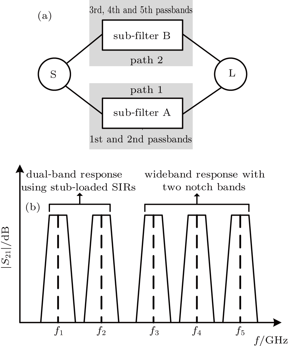
Figure 1(a) shows the basic coupling scheme diagram of the proposed quint-band superconducting BPF. In the lower path, four stub-loaded SIRs are used to implement a dual-band response, forming the 1st and 2nd passbands. While in the upper path, seven resonators are used to construct a wideband response which two notch bands are introduced into, thus the 3rd, 4th, and 5th passbands are established. Then, a new impedance matching junction is utilized to combine the two sub-filters mentioned above into a quint-band BPF. This method can make the complexity of designing matching junctions and size reduced considerably, compared with the traditional method which combines five sub-filters with common I/O ports. The response of the quint-band BPF is simply illustrated in Fig. 1(b), where the center frequencies of the five passbands are located at 2.4, 3.5, 4.7, 5.3, and 5.9 GHz, respectively.

Fig. 1. (a) Coupling scheme diagram of the proposed quint-band BPF. (b) Frequency response of quint-band BPF with five passbands contributed by two sub-filters.
2.1. Sub-filter A of lower path: 1st and 2nd passbands

In the lower path of the quint-band filter, the first two passbands are constructed by four SL-SIRs. The simulated frequency responses, and current density distribution[23] of the SL-SIR are obtained and shown in Figs. 2(a) and 2(b). The Sonnet full-wave electromagnetic (EM) simulation is used in this paper.
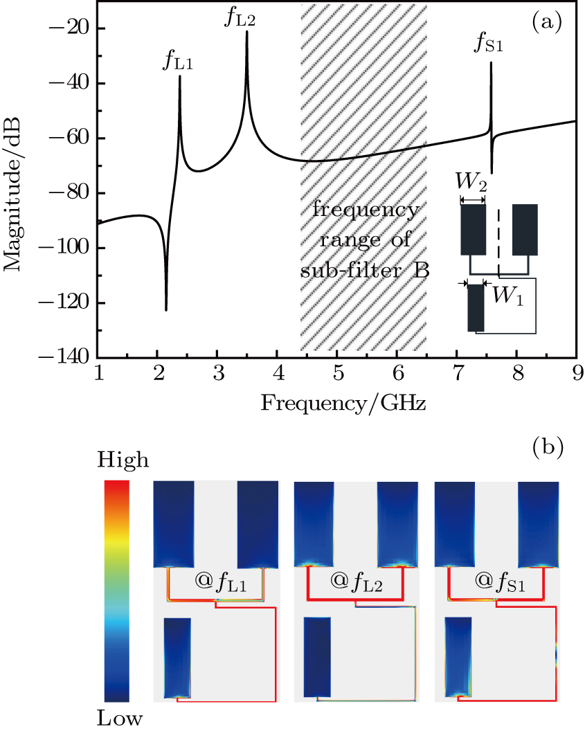
Fig. 2. (color online) (a) Simulated resonant frequency response of the SL-SIR. (b) Simulated current density distribution of the SL-SIR at resonant frequencies of fL1, fL2, and fS1.

The first two resonant modes generated by the SL-SIR are denoted as fL1 and fL2, and the first spurious frequency is represented by fS1. The current is distributed on the entire resonator at fL1, while it concentrates mainly on the upper part at fL2. Given that the open stub is shunted at the midpoint of the U-type SIR, the odd- and even-mode analysis can be adopted to characterize resonant modes. The lower frequency fL1 corresponds to the even mode, while fL2 corresponds to the odd mode.[24] Figures 3(a) and 3(b) show that the extracted resonant frequencies change with W1 and W2, respectively. Moreover, fL2 can be adjusted by altering W2, whereas fL1 varies slightly. When W1 is changed, only fL1 is shifted, while fL2 remains fixed. Therefore, the frequencies of the first two passbands can be independently controlled. Finally, the width of W2 is set to be 1.32 mm and W1 is adopted to be 0.86 mm, so that fL1 and fL2 are fixed to be 2.4 GHz and 3.5 GHz, respectively. fS1 is pushed up to 7.5 GHz to prevent it interfering with the last three passbands.
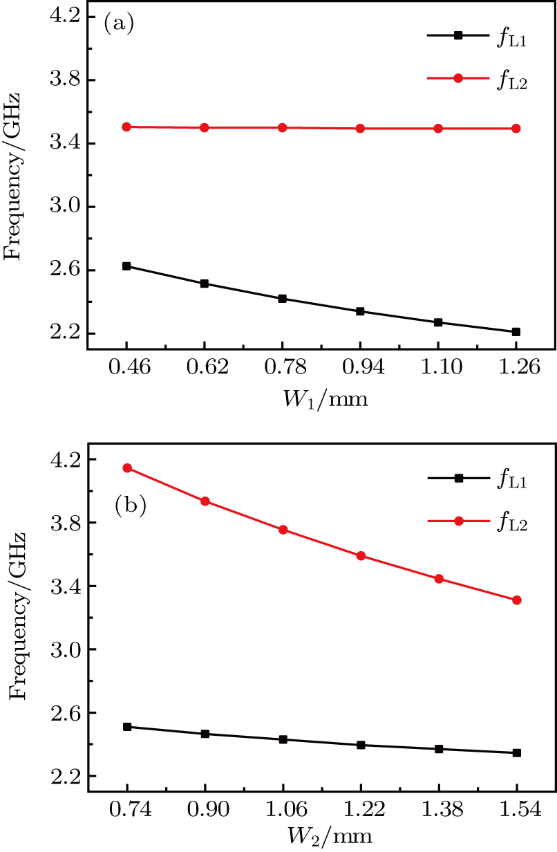
Fig. 3. (color online) (a) Extracted resonant frequencies varying with W1 with W2 being set to be 1.32 mm. (b) Extracted resonant frequencies varying with W2 with W1 being set to be 0.86 mm.

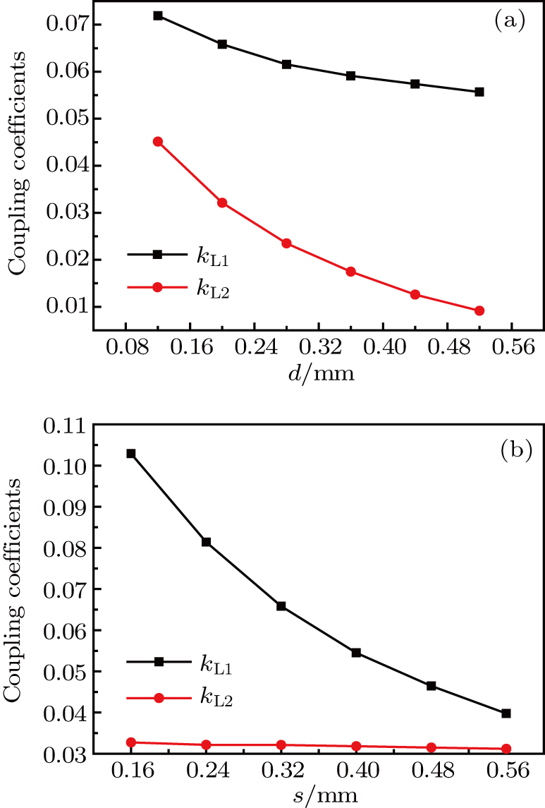
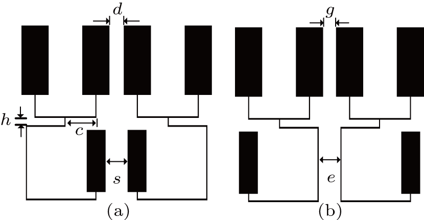
Figures 5(a) and 5(b) show the plots of the simulated coupling coefficients versus distance between the U-type SIRs, d, and the folded open stubs, s, respectively, where kL1 and kL2 represent the couplings at fL1 and fL2 respectively. Parameters c and h are tuned to keep the frequencies fL1 and fL2 unchanged. The coupling coefficients of the structure in Fig. 4(b) can be derived in the same way. Figure 5(a) shows that parameter d affects both kL1 and kL2 when s is fixed, while figure 5(b) indicates that parameter s has a large influence on kL1 but affects kL2 less when d is fixed. Thus, the coupling strengths kL1 and kL2 can be controlled separately.

Fig. 4. Two kinds of coupling structures (not to scale).
Fig. 5. (color online) Simulated coupling coefficients in Fig. 4(a) varying with (a) d (s is fixed at 0.32 mm) and (b) s (d is fixed at 0.2 mm) for kL1 and kL2.

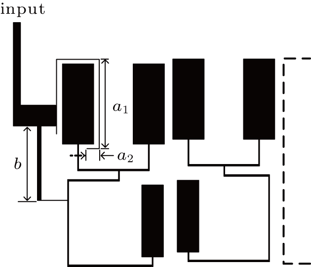
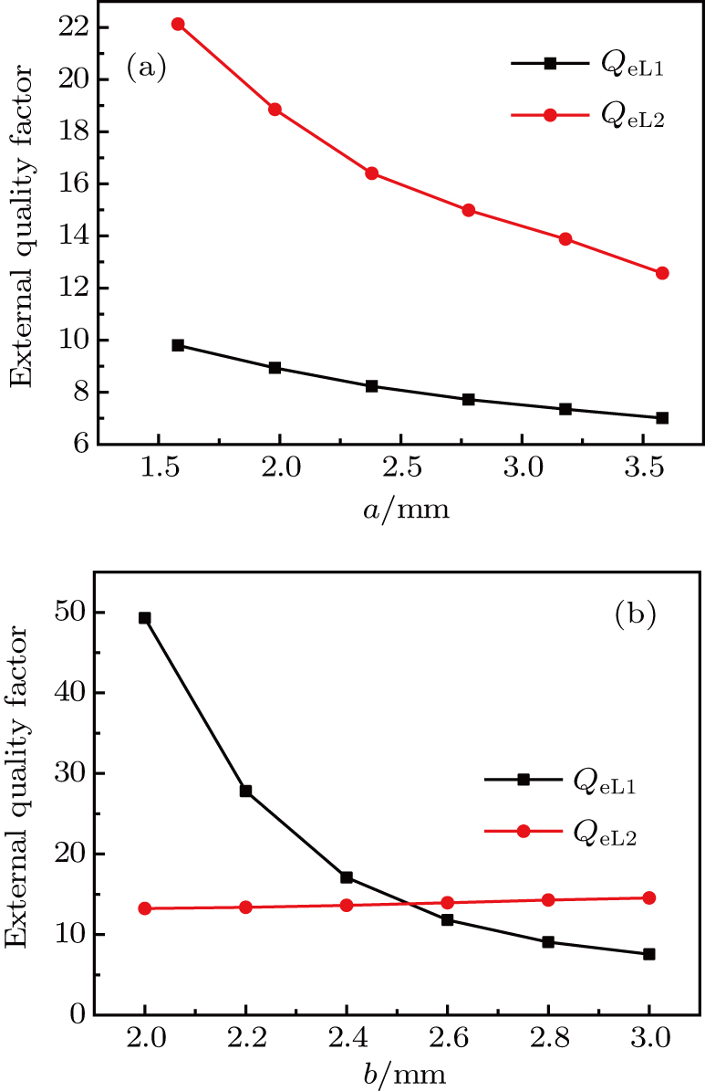
Figure 6 shows the dual-feeding external coupling structure of sub-filter A. One branch is spiraled around the end of the U-type SIR, and the other branch is tapped to the open stub. Figure 7(a) shows the external quality factors QeL1 at fL1 and QeL2 at fL2 decrease as coupling length a increases. While as tap position parameter b increases, QeL1 decreases rapidly whereas QeL2 increases slightly in Fig. 7(b). Parameters a and b are appropriately combined to meet the required external coupling of the two passbands simultaneously. Therefore, the center frequencies and bandwidths of the first two passbands can be controlled.

Fig. 6. Layout of the sub-filter A (not to scale).
Fig. 7. (color online) Simulated external quality factors for the first two passbands varying with (a) a (b is fixed at 3.0 mm), and (b) b (a is fixed at 2.98 mm. a = a1 + a2).
2.2. Sub-filter B of upper path: 3rd, 4th, and 5th passbands

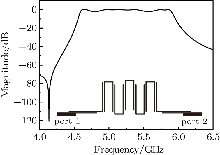
In the upper path of the quint-band filter, two notch bands are introduced into a wideband response. Seven resonators are used to construct the wideband response. The first and last resonator are transformed into L-type resonators to excite stronger external coupling to the ports, while the rest of the resonators are all hairpin resonators. The basic wideband response is shown in Fig. 8.

Fig. 8. Wideband response constructed by L-type and hairpin resonators.

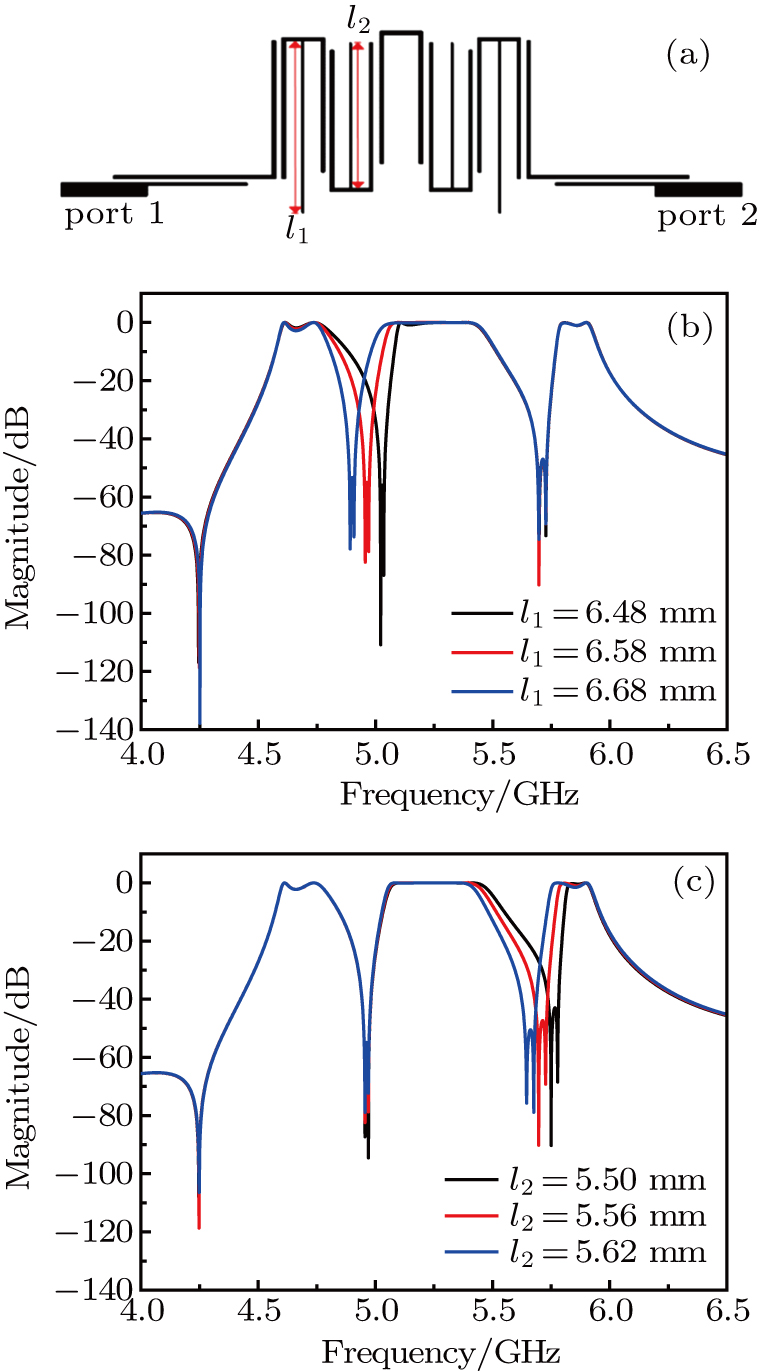
Two pairs of stubs of different lengths are loaded in the middle of the hairpin resonators, introducing two notch bands as shown in Fig. 9. The notch bands can be controlled by adjusting the lengths of the stubs. Figure 9(b) shows that the first notch band is shifted to a lower frequency as length l1 increases, while the second notch band remains fixed. Moreover, figure 9(c) shows the shift of the second notch band with the change of the length l2, similarly. Therefore, the central frequencies and bandwidths of the three passbands can be adjusted.

Fig. 9. (color online) (a) Layout of the filter. (b) Simulated frequency responses with varying l1 (l2 is set to be 5.56 mm). (c) Simulated frequency responses with varying l2 (l1 is set to be 6.58 mm).
2.3. Structure of matching junctions and filter design

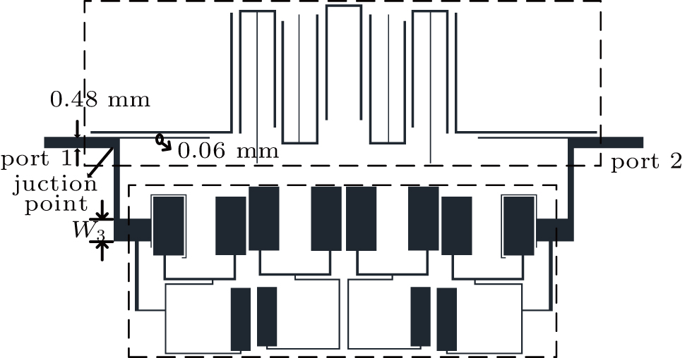
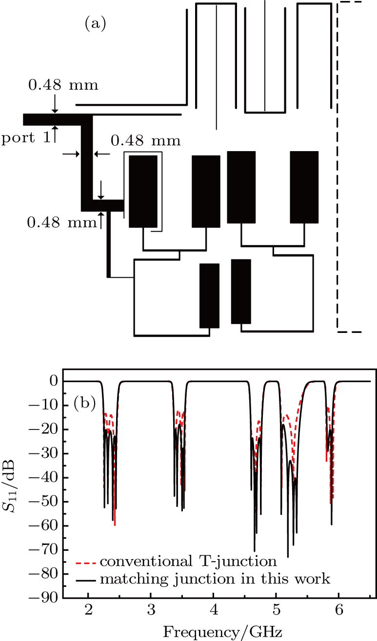
Figure 10 shows the layout of the proposed quint-band filter consisting of two sub-filters connected by matching junctions. The first two passbands are integrated by a T-junction to form the sub-filter A. Then, a T-junction is used to connect the two sub-filters to the common I/O ports. The horizontal branch line of the T-junction with a small width of 0.06 mm is used to achieve a strong capacitive external coupling of sub-filter B. On the other hand, the vertical branch line is connected to the sub-filter A with a short horizontal branch line with width W3.

Fig. 10. Layout of the quint-band filter. The circuit in the lower dashed rectangular box shows sub-filter A, and the upper shows sub-filter B. W3 is the width of branch line connecting to the matching junction.

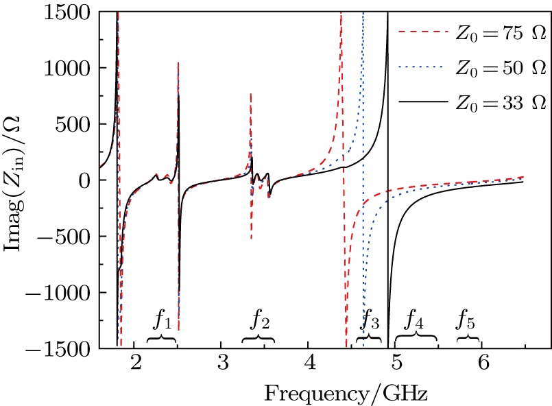
Figure 11 shows the effect of adjusting W3. The plots of the simulated imaginary part of input impedance Zin versus frequency of the sub-filter A at the junction point with different values of characteristic Z (33, 50, and 75 Ω) are presented. The simulation layout of sub-filter A is shown in Fig. 6. Zin is matched to 50 Ω in passbands 1 and 2, having a nonzero imaginary part in each of passbands 3, 4, and 5, which introduces a strong interaction between the sub-filters. The ideal conditions for Zin of the sub-filter A can be illustrated as follows:

The five passbands are denoted as f1, f2, f3, f4, and f5, respectively. As the absolute values of Zin at f3, f4, and f5 increase, the interaction between the sub-filters decreases. Moreover, when the out-of-band signals are inputted from the common port, Zin = ∞ means that the sub-filter A acts as an open circuit. It can be seen that as W3 widens, the peak of the nonzero part is pushed to a higher frequency. Finally, width W3 is set to be 0.98 mm to increase the imaginary part of Zin of the sub-filter A in each of passbands 3, 4, and 5, so that the interaction between the two sub-filters can be reduced. Compared with the conventional T-junction shown in Fig. 12(a), the stepped-impedance matching junctions used in this work possess better frequency response, as indicated in Fig. 12(b).

Fig. 11. (color online) Plots of simulated Imag (Zin) versus frequency of sub-filter A with different characteristic impedances (Z0 = 33, 50, and 75 Ω, corresponding to width W3 = 0.98, 0.48, and 0.18 mm).
Fig. 12. (color online) (a) Layout of the filter using conventional T-junction (not to scale). (b) Simulated results of the filters using conventional T-junction and matching junctions proposed in this work.

The two sub-filters are designed by adopting different structures of resonators, and the shortest distance between the two sub-filters is pulled away to 1 mm, so the cross-coupling can be weakened. Afterwards, the parameters of the quint-band filter, including the resonant frequencies, the external and interstage couplings, and the lengths of the matching branch lines, are optimized entirely to minimize further the undesired interactions and achieve a better filter response.

3. Fabrication and experimental performance

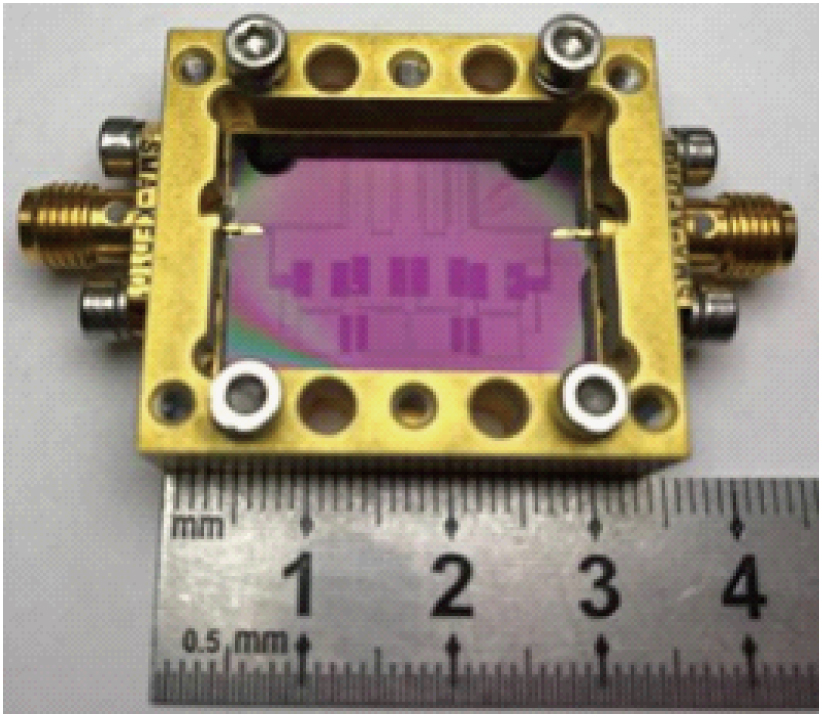
The quint-band HTS filter is fabricated on double-sided YBCO films deposited on a 0.5-mm-thick MgO substrate. The ion etching technology is used to etch one-side of the film to form the filter circuit. The filter is then packaged into a gold-plated shield box with an overall size of 26 mm × 19 mm, or 0.51λg × 0.37λg, where λg is the guided wavelength at the central frequency of the first passband. Figure 13 shows the photograph of the fabricated quint-band filter with an open cover. The filter is cooled to 65 K through a Stirling cryocooler and measured by an Agilent E5072 A network analyzer with an input power of 0 dBm.

Fig. 13. (color online) Photograph of fabricated HTS filter.

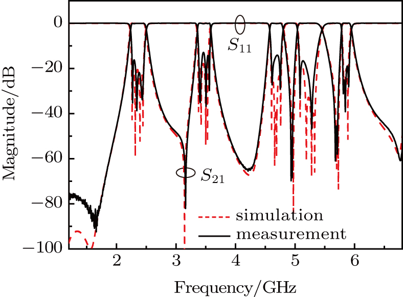
Figure 14 presents the measured results of the quint-band HTS filter without tuning, which accord well with the simulations. The measured results of the five passbands are listed in Table 1. The insertion loss of the five passbands is less than 0.25 dB, and the return loss is greater than 13 dB. The rejection of the four internal stopbands is higher than 45 dB.

Fig. 14. (color online) Simulated and measured results of the quint-band HTS filter.
Table 1.

Measurements of the quint-band BPF.

.
4. Conclusions

Two high-pole multiband sub-filters have been constructed by adopting different structures and then used to determine a compact quint-band filter with controllable frequencies and bandwidths. The interaction between the sub-filters is reduced by the matching junctions with branch lines, which have different characteristic impedances. Experiments demonstrate that the designed and fabricated filter shows good return loss and low insertion, which matches well with the simulations.

Reference
[1] Zuo T Zhao X J Wang X K Yue H W Fang L Yan S L 2009 Acta Phys. Sin. 58 4194 in Chinese
[2] Zhang Q S Zhu F J Zhou H S 2015 Chin. Phys. 24 107506
[3] Liu X Y Zhu L Feng Y J 2016 Chin. Phys. 25 034101
[4] Me C M Xu J Kang W Wu W 2016 Electron. Lett. 52 1463
[5] Ai J Zhang Y H Xu K D Li D T Fan Y 2016 IEEE Microw. Wireless Compon. Lett. 26 343
[6] Hsu K W Lin J H Tu W H 2014 IEEE Microw. Wireless Compon. Lett. 24 593
[7] Chen S F 2012 IEEE Microw. Wireless Compon. Lett. 22 357
[8] Heng Y Guo X B Cao B S Wei B Zhang X P Chen W Ying Z J Song X K 2013 Electron. Lett. 49 658
[9] Wu H W Yang R Y 2011 IEEE Microw. Wireless Compon. Lett. 21 203
[10] Cui C W Liu Y 2014 Electron. Lett. 50 1719
[11] Ren L Y 2010 IEEE Microw. Wireless Compon. Lett. 20 429
[12] Bukuru D Song K J Zhang F Zhu Y Fan M Y 2017 IEEE Trans. Microw. Theory Tech. 65 783
[13] Wei F Qin P Y Guo Y J Shi X W 2016 IET Microw. Anten. Propag. 10 230
[14] Xu J Wu W Miao C 2013 IEEE Trans. Microw. Theory Tech. 61 3187
[15] Gao L Zhang X Y Zhao X L Zhang Y Xu J X 2016 IEEE Microw. Wireless Compon. Lett. 26 395
[16] Zhang Y Gao L Zhang X Y 2015 IEEE Microw. Wireless Compon. Lett. 25 645
[17] Xu J 2015 Microw. Opt. Technol. Lett. 57 997
[18] Xiao M Li X Z Sun G L 2016 Electron. Lett. 52 848
[19] Wei F Shi X W 2014 Microw. Opt. Technol. Lett. 56 1633
[20] Liu J C Wang J W Zeng B H Chang D C 2010 IEEE Microw. Wireless Compon. Lett. 20 142
[21] Song F Zhu L Wei B Cao B S Jiang L N Li B 2016 IEEE Trans. Appl. Supercond. 26 1501610
[22] Liu H W Ren B P Guan X H Wen P Wang Y 2014 IEEE Trans. Microw. Theory Tech. 62 2931
[23] Heng Y Guo X B Cao B S Wei B Zhang X P Zhang G Y Song X K 2013 IEEE Microw. Wireless Compon. Lett. 23 400
[24] Lu X L Wei B Cao B S Guo X B Zhang X P Song X K Heng Y Xu Z 2014 IEEE Trans. Appl. Supercond. 24 1500205