Superconductivity of bilayer titanium/indium thin film grown on SiO2/Si (001)
Mo Zhao-Hong1, 2, Lu Chao1, Liu Yi1, Feng Wei1, Zhang Yun1, Zhang Wen1, Tan Shi-Yong1, Zhang Hong-Jun1, Guo Chun-Yu3, Wang Xiao-Dong1, Wang Liang1, Yang Rui-Zhu1, Ren Zhong-Guo1, Zhu Xie-Gang1, †, Xiong Zhong-Hua1, An Qi2, Lai Xin-Chun4, ‡
Institute of Materials, China Academy of Engineering Physics, Jiangyou 621908, China
Department of Engineering and Applied Physics, School of Physical Sciences, University of Science and Technology of China, Hefei 230026, China
Zhejiang University, Hangzhou 310058, China
China Academy of Engineering Physics, Mianyang 621000, China


† Corresponding author. E-mail: zhuxg02@gmail.com laixinchun@caep.cn

Abstract

Bilayer superconducting films with tunable transition temperature (Tc) are a critical ingredient to the fabrication of high-performance transition edge sensors. Commonly chosen materials include Mo/Au, Mo/Cu, Ti/Au, and Ti/Al systems. Here in this work, titanium/indium (Ti/In) bilayer superconducting films are successfully fabricated on SiO2/Si (001) substrates by molecular beam epitaxy (MBE). The success in the epitaxial growth of indium on titanium is achieved by lowering the substrate temperature to −150 °C during indium evaporation. We measure the critical temperature under a bias current of 10 μA, and obtain different superconducting transition temperatures ranging from 645 mK to 2.7 K by adjusting the thickness ratio of Ti/In. Our results demonstrate that the transition temperature decreases as the thickness ratio of Ti/In increases.

PACS: 74.78.-w;
1. Introduction

A transition edge sensor (TES) is a superconducting thin film biased in the transition region from the superconducting to the normal state, and serves as a sensitive thermometer that relies on the steep resistive transition of a superconducting material. Because of its high thermal sensitivity, it has wide applications in many areas, including single photon detectors from near-infrared to γ-ray, cosmic microwave background bolometers, and dark matter detectors.[115] The Tc of a bilayer superconducting thin film system could be tuned in a well controlled way by just tuning the thickness ratio of the two elements. Many bilayer systems, such as Mo/Au, Mo/Cu, Ti/Au, and Ti/Al systems,[1,11,1621] have been chosen for fabricating the TESs.

Two techniques are in common use for depositing the high-quality bilayers: (i) e-beam evaporation and (ii) sputtering deposition. While in principle the fabrication of bilayer thin films should be quite straightforward, in practice its reproducibility remains a significant challenge, because it is difficult to control and disentangle in the individual contributions (strain, crystalline structure, contamination) in the above mentioned fabrication process. The state-of-the-art molecular beam epitaxy (MBE) technique offers a better option in the fabrication of bilayer thin films. During the MBE growth, the deposition rate can be monitored by quartz crystal micro-balance (QCM) and controlled within an accuracy of less than 0.01 nm/s. In the ultra-high vacuum (UHV) environment (≈ 1.0 ×10⁻¹⁰ mbar, 1 bar = 105 Pa), by appropriately controlling the substrate temperature and deposition rate, the reproducibility of the quality of the bilayer thin films could be guaranteed by the MBE technique.

In this work, we study the superconductivity of a new bilayer system, i.e., Ti/In thin film, aiming at developing a new TES. Theoretically, Tc of the Ti/In bilayer can be tuned between 390 mK (Tc of Ti bulk) and 3.4 K (Tc of indium bulk), where the Ti layer serves as the normal metal. We fabricate Ti/In bilayers by MBE to ensure the cleanliness of the interface and controllable thickness ratio. We successfully tune the Tc of Ti/In bilayer thin films from 645 mK to 2.7 K by adjusting the thickness ratio. The lowest Tc (645 mK) in our work is a little higher but also comparable to the results of the Al/Ti bilayer in Refs. [1] and [11] whose lowest Tc is around 540 mK. This implies that it is possible for our sample to be used as TES bolometers for millimeter wave and submillimeter wave astrophysics.

2. Experiments and methods

In order to study the superconductivities of Ti/In superconducting thin films, various thickness ratios of Ti/In were primarily deposited on 300-nm SiO2 on a ⟨100⟩ monocrystalline silicon substrate. The Ti/In films grew on a molecular beam epitaxial apparatus at a base pressure better than 1.0 × 10⁻¹⁰ mBar. High-purity indium (5 N) and titanium (5 N) were used for the growth. The temperature of the indium and titanium sources were kept at 750 °C and 1610 °C, respectively. For the growth of titanium film, the substrate was kept at 80 °C, while it was at −150 °C for the indium film growth. The detailed optimized growth conditions are listed in Table 1.

Table 1.

In/Ti film production parameters.

.

Scanning electron microscopy (SEM) was performed with an energy dispersive spectrometer (EDS) to characterize the surface morphology and the element compositions of the grown thin films. A physical property measurement system (PPMS) was used to study the superconductivities of the thin films.

3. Results and discussion
3.1. Effect of growth temperature on In thin film

The growth temperature is a critical parameter which can affect the quality of the film grown by MBE. The temperature affects the adhesion coefficient, growth rate, background impurity density, doping conditions, surface morphology, and interface between different epitaxial layers. The experiments were carried out under different temperature conditions.

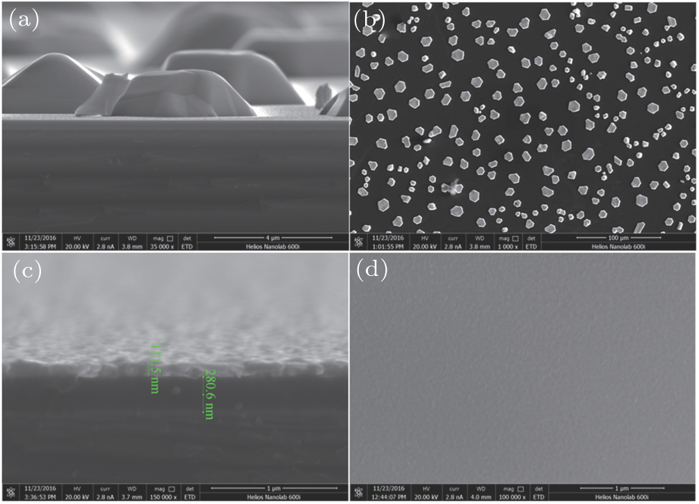
Figures 1(a) and 1(b) show the cross section morphology and surface morphology of indium on the 50-nm thick titanium film without changing the temperature of the substrate in the whole growth process. Indium atoms migrate into islands with diameters in a range from 1 μm to 9 μm, spacings in a range from 10 μm to 20 μm and heights of about 1 μm. This sample shows no sign of superconductivity in the resistance measurement. To the best of our knowledge, there is currently no other work on indium-related bilayer systems for TES applications, which might be because of the difficulty in the growth of continuous indium thin film at high ambient temperature. Figures 1(c) and 1(d) show the cross section morphology and surface morphology of the In film that grew on Ti with the substrate temperature being −150 °C. It is obvious that the growth mode is changed from island-like to layer-by-layer film-like, as the substrate temperature decreases to a low temperature. This can be qualitatively explained by the evolution of the diffusion rate of indium atoms on the titanium surface with temperature. For the temperatures in Figs. 1(a) and 1(b), the indium atoms have fast diffusion rates and migrate into sparsely distributed islands. Under low temperatures, the indium atoms move across the titanium film more slowly and tend to condense into film due to the cohesion between indium atoms.

Fig. 1. (color online) (a) Cross section morphology and (b) surface morphology of Ti/In bilayer thin film grown at constant substrate temperature; (c) cross section morphology, and (d) surface morphology of Ti/In bilayer thin film with indium layer grown at −150 °C and Ti layer grown at 80 °C.
3.2. Superconductivity measurement

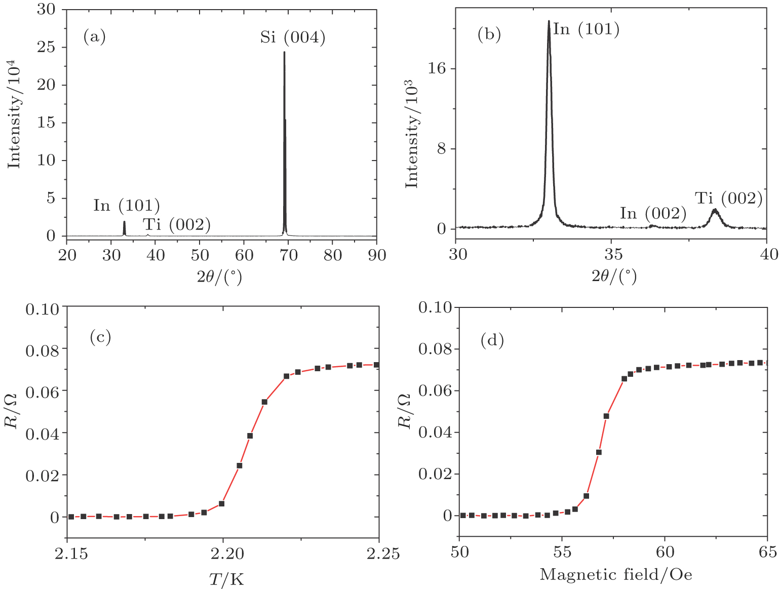
We refer to the first successfully fabricated superconducting bilayer Ti/In film as sample #1, in which the indium layer is deposited at low temperature (−150 °C). The thickness values of titanium and indium layers are 100 nm and 130 nm, respectively. Figures 2(a) and 2(b) show the XRD results of sample #1. The XRD intensity of the (004) peak of the Si substrate dominates in Fig. 2(a). The detailed structural information of our Ti/In film is revealed in Fig. 2(b). Only the (002) diffraction peak of titanium is observed, which means that the direction of titanium thin film is mainly along the (001) direction. However, the indium thin films crystalize along the (101) and (001) directions. Our XRD results indicate that the Ti/In thin films are not just randomly oriented amorphous layers, but well-oriented and crystalized thin films with good quality.

Fig. 2. (color online) ((a) and (b)) X-ray diffraction (XRD) results, (c) resistance–temperature (RT) curve, (d) resistance–magnetic field curve of sample #1 (sample #1 is the first Ti/In bilayer that was successfully fabricated). The unit 1 Oe = 79.5775 A · m−1.

Figures 2(c) and 2(d) show respectively the resistance-temperature and resistance-magnetic field curves of sample #1, measured by PPMS. The superconducting transition temperature (Tc) of sample #1 is 2.228 K with a transition width (ΔTc) of 27 mK and the critical magnetic field is 57 Oe (1 Oe = 79.5775 A·m−1) at 2 K. It should be noted that the Tc of bulk indium is about 3.4 K, and it was reported that a remarkable increase of Tc was observed as the thickness of indium thin film decreased.[22] However, our Ti/In bilayer thin film has a Tc of 2.228 K, which is far less than the bulk Indium, despite the fact that the thickness of our Indium layer is merely 130 nm. These unconventional results could be explained by the proximity effect[17,23] between normal metal and superconducting metal. Here in our work, indium serves as a superconducting metal, while the titanium layer is used as a normal metal. The above results imply that it is possible to tune the superconducting transition temperature by adjusting the thickness ratio of Ti/In layers.

3.3. Superconductivities of thin films with various Ti/In thickness ratios

To study the manipulation of the transition temperature ratio of Ti/In (k), a series of Ti/In bilayer samples with various thickness ratio is fabricated and their transport properties are characterized systematically and shown in Fig. 3. The thickness values of indium layers in the series are kept at a constant of 129.6 nm. We obtain different thickness ratios by changing the thickness of the titanium layer. Due to the proximity effect, Tc decreases monotonically as the thickness of Ti layer increases, i.e., k, which is the thickness ratio of titanium to indium, increases. A similar phenomenon is also observed in the critical magnetic field measurement. The superconducting gap of the indium layer is suppressed due to the titanium layer (which serves as a normal metal) by an inverse proximity effect.[23,24] According to the Bardeen–Cooper–Schrieffer (BCS) theory,[25]Tc is a function of the superconducting gap expressed as where Δ(0) is the superconducting gap at 0 K. Therefore, as the superconducting gap of the indium layer is suppressed gradually, the Tc of the film decreases.

Fig. 3. (color online) (a) Resistance–temperature curves and (b) resistance–magnetic field curves for bilayer samples with various Ti/In ratios, with insets indicating the values of thickness ratio (k = dTi/d In).

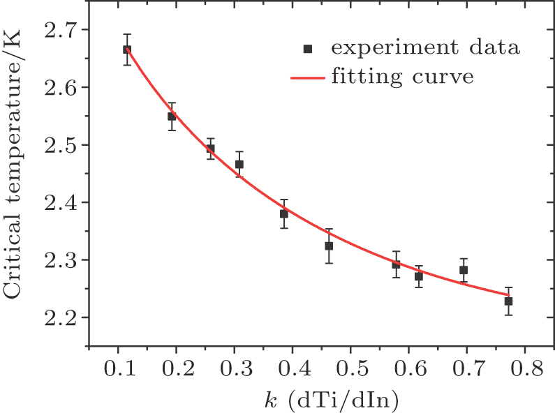
Figure 4 shows the evolution of the measured Tc with thickness ratio k, which demonstrates explicitly the decrease of Tc as k increases. Empirically, the Tc of a composite superconducting and normal metal layer can be described as[23,26] where and In the above relationship, λF is the Fermi wavelength, the subscript S refers to the superconducting film and N denotes the normal metal film making up the bilayer, dN is the thickness of normal metal film, dS is the thickness of superconducting film, nN is the density of states of normal metal film, and nS is the density of states of superconducting film. Parameter t is a transmission factor and Tc,S is the transition temperature of superconducting metal film.

Fig. 4. (color online) Tck curve.

In our work, dS = 129.6 nm. We define k = dN/dS = dN/129.6. It is assumed that titanium is a normal metal when temperature is above 390 mK, which is the Tc value of the titanium bulk, and that the other constant terms appear in the empirical formula (2), which gives the following fitting formula: where A, B, and C are constant parameters. The fitted curve is shown in Fig. 4, with A = 0.55633, B = 2.97684, and C = 0.34189, which matches the experimental data quite well.

To check the validity of the above model (Eq. (2)), a new empirical Tck curve shown in Fig. 5(a) is derived by changing dS from 129.6 nm to 50 nm. A Ti (300 nm)/In (50 nm) bilayer thin film, which corresponds to k = 6, is fabricated and the value of Tc is measured to be about 645 mK, which is a little higher than the theoretical Tc (500 mK). We think that the discrepancy in Tc might be due to the general non-uniformity in the thickness of indium films, which could be seen from Figs. 1(c) and 1(d). Usually, the annealing of grown thin film will result in a well-ordered and flat surface. Therefore, for future work on improving the quality of the indium films and thus reducing the Tc, we will try various annealing temperatures and check their effects on the surface morphologies and Tc values of Ti/In bilayers.

Fig. 5. (color online) (a) Tck curve (black solid curve) derived from the formula (5) and the datum of Ti (300 nm)/In (50 nm) (red point), (b) RT curve of Ti (300 nm)/In (50 nm).
4. Conclusions

Superconducting Ti/In bilayer thin films are successfully fabricated on SiO2/Si (001) substrate. The key issue for the growth process of the indium layer is to keep the substrate at a low temperature of −150 °C. Based on the proximity effect, the transition temperature Tc and the critical magnetic field of the Ti/In film are manipulated continuously by changing the thickness ratio k of the Ti/In layer. An empirical relationship between Tc and k based on the BCS theory is adapted to qualitatively explain the observed results. The validity of the empirical relationship is also checked experimentally, which implies the vast possibilities of manipulating the Tc of the Ti/In bilayer system, or other superconducting/normal layer systems by proximity effects. More researches on tuning the Tc of the Ti/In bilayer to even lower temperature and the possible application to practical TES sensors are under way.

Reference
[1] Zhang Q Y Liu J S Dong W H Wang T S He G F Li T F Zhou X X Chen W 2014 Chin. Sci. Bull. 59 2292
[2] Zhang L Zhao Q Zhong Y Chen J Cao C Xu W Kang L Wu P Shi W 2009 Appl. Phys. 97 187
[3] Liu J Zhang L Q Jiang Z N Ahmad Kamal Liu J S Chen W 2016 Chin. Phys. Lett. 33 088502
[4] Liu X Guo W Wang Y Dai M Wei L F Dober B McKenney C M Hilton G C Hubmayr J Austermann J E Ullom J N Gao J Vissers M R 2017 Appl. Phys. Lett. 111 252601
[5] Guo S B Zhong K Wang M R Liu C Xiao Y Wang W P Xu D G Yao J Q 2017 Chin. Phys. 26 019501
[6] Wang T S Chen J K Zhang Q Y Li T F Liu J S Chen W Zhou X 2013 Nucl. Instrum. Methods Phys. Res. 729 474
[7] Li H Wang Y Wei L Zhou P Wei Q Cao C Fang Y Yu Y Wu P 2013 Chin. Sci. Bull. 58 2413
[8] Na Z Liu J S LI H LI T F Chen W 2012 Chih. Phys. Lett. 29 088401
[9] You L X Shen X F Yang X Y 2010 Chin. Sci. Bull. 55 441
[10] Wang J P Li Y B Kang L Wang Y Zhong Y Y Liang M Chen J Cao C H Xu W W Wu P H 2009 Chin. Sci. Bull. 54 2013
[11] Zhang Q Y Wang T S Liu J S Dong W H He G F Li T F Zhou X X Chen W 2014 Chin. Phys. 23 118502
[12] Guo W Liu X Wang Y Wei Q Wei L F Hubmayr J Fowler J Ullom J Vale L Vissers M R Gao J 2017 Appl. Phys. Lett. 110 212601
[13] Zhou P J Wang Y W Wei L F 2014 Chih. Phys. Lett. 31 067402
[14] He Y H Lv C L Zhang W J Zhang L Wu J J Chen S J You L X Wang Z 2015 Chin. Phys. 24 060303
[15] Zhang C Jiao R Z 2012 Chin. Phys. 21 120306
[16] Jaeckel F T Kripps K L Morgan K M Zhang S McCammon D 2016 J. Low Temp. Phys. 184 647
[17] Wang G Yefremenko V Chang C L Novosad V Mehl J Pearson J Divan R Carlstrom J E 2013 IEEE Trans. Appl. Supercond. 23 2101605
[18] Glowacka D M Goldie D J Withington S 2010 21st International Symposium on Space Terahertz Technology March 23–25, 2010 Oxford 276
[19] Gonzalez-Arrabal R Camón A Parra-Borderías M Fabrega L Anguita J Sesé J Briones F 2008 J. Low Temp. Phys. 151 239
[20] Ali Z A Drury O B Cunningham M F Chesser J M T W B Jr Friedrich S 2005 IEEE Trans. Appl. Supercond. 15 526
[21] Olsen J Kirk E C Thomsen K Brandt V D Lerch P Scandella L Zehnder A Mango S Ott H R Huber M Hilton G C Martinis J M 2000 Nucl. Instrum. Methods Phys. Res. 444 253
[22] Toxen A M 1961 Phys. Rev. 123 442
[23] Sadleir J E 2010 Superconducting Transition-edge Sensor Physics Ph. D. Dissertation Illinois University of Illinois at Urbana-Champaign
[24] Yu H L Dong Z C 2007 Chin. Phys. 16 3072
[25] Bardeen J Cooper L N Schrieffer J R 1957 Phys. Rev. 106 162
[26] Martinis J M Hilton G C Irwin K D Wollman D A 2000 Nucl. Instrum. Methods Phys. Res. 444 23