Polycrystalline cubic boron nitride prepared with cubic-hexagonal boron nitride under high pressure and high temperature
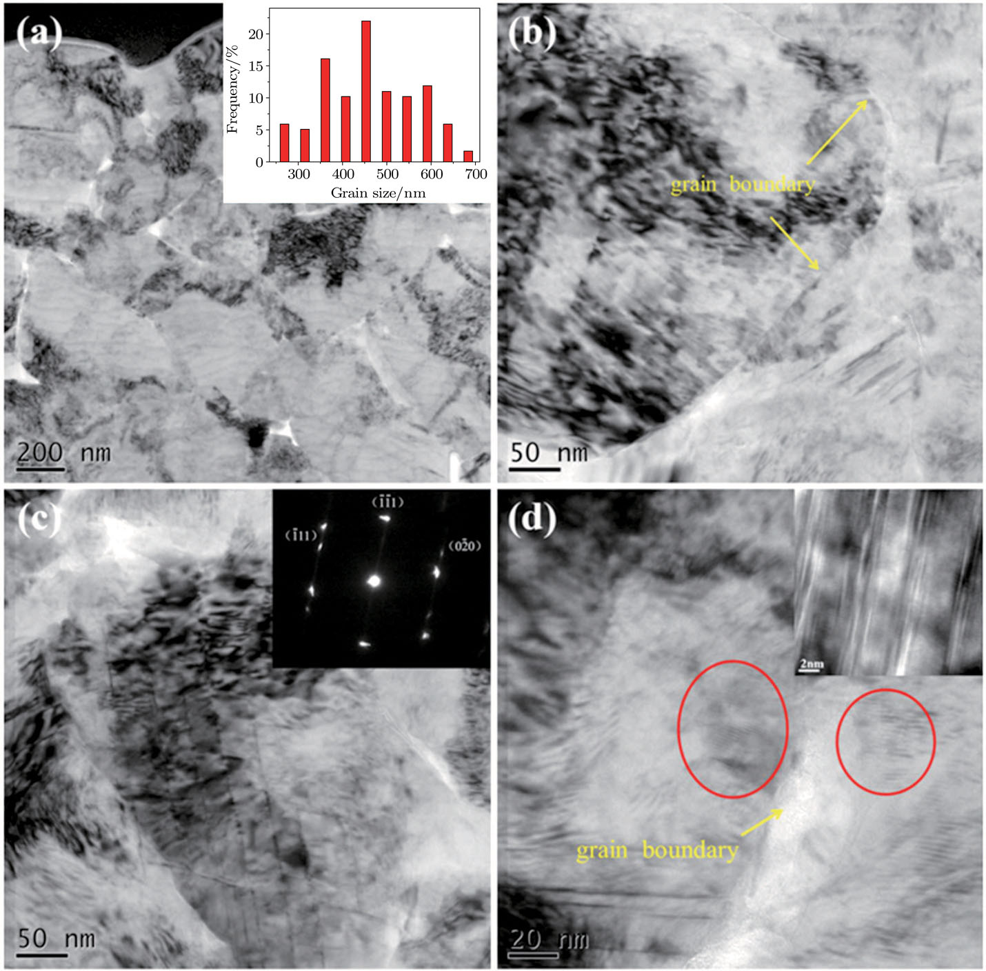
(color online) TEM characterization of sample sintered at 7.7 GPa/1750 °C. (a) TEM image of the submicron cBN sample covers several grains. Upper-right inset: size distribution of grains measured from TEM images with an average grain size of ∼450 nm. (b) The grain boundary is observed as a circular arc. (c) TEM image of the interaction of a grain exhibiting numerous nanotwins. Upper-right inset: corresponding selected area electron diffraction pattern. (d) TEM image showing a large number of defects in the pure cBN sample. Upper-right inset: HRTEM image of stacking faults inside a grain.
