Gap plasmon-enhanced photoluminescence of monolayer MoS2 in hybrid nanostructure
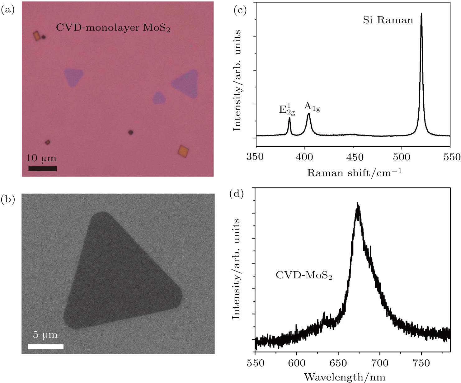
(color online) (a) and (b)) Optical microscope (OM) and scanning electron microscope (SEM) images of the CVD-grown MoS2 deposited on SiO2/Si substrate. (c) Raman spectrum of CVD-MoS2. (d) Typical PL spectrum of MoS2 showing a strong emission peak at ∼670 nm.