An overview of thermoelectric films: Fabrication techniques, classification, and regulation methods
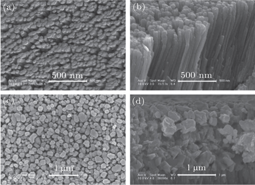
(color online) SEM images of a ternary compound n-type Bi2(Te,Se)3 films [(a) and (b)] ordered nanowire array and [(c) and (d)] ordinary films with [(a) and (c)] surface view, (b) oblique view, and (d) cross-sectional view.[