Zhang Zhenzhen, Fu Zhanglong, Guo Xuguang, Cao Juncheng. 4.3 THz quantum-well photodetectors with high detection sensitivity. Chinese Physics B, 2018, 27(3): 030701
Permissions
4.3 THz quantum-well photodetectors with high detection sensitivity
Zhang Zhenzhen1, 3, Fu Zhanglong1, Guo Xuguang2, Cao Juncheng1, †
Key Laboratory of Terahertz Solid-State Technology, Shanghai Institute of Microsystem and Information Technology, Chinese Academy of Sciences, Shanghai 200050, China
Ministry of Education and Shanghai Key Laboratory of Modern Optical System and Shanghai Terahertz Research Center, University of Shanghai for Science and Technology, Shanghai 200093, China
University of Chinese Academy of Sciences, Beijing 100049, China
We demonstrate a high performance GaAs/AlGaAs-based quantum-well photodetector (QWP) device with a peak response frequency of 4.3 THz. The negative differential resistance (NDR) phenomenon is found in the dark current–voltage (I–V) curve in the current sweeping measurement mode, from which the breakdown voltage is determined. The photocurrent spectra and blackbody current responsivities at different voltages are measured. Based on the experimental data, the peak responsivity of 0.3 A/W (at 0.15 V, 8 K) is derived, and the detection sensitivity is higher than 1011 Jones, which is in the similar level as that of the commercialized liquid-helium-cooled silicon bolometers. We attribute the high detection performance of the device to the small ohmic contact resistance of and the big breakdown bias.
Terahertz quantum well photodetectors (THz QWPs) based on intersubband transitions extend the operation wavelength of quantum-well infrared photodetectors from mid-infrared to terahertz regime.[1–3] They are important components for terahertz imaging and terahertz free space communication due to their distinctive advantages of high sensitivity and fast response. The maturity of III–V compound semiconductor material growth and processing techniques makes it possible to fabricate high uniformity, excellent reproducibility, large area, and low-cost imaging arrays.[4–8] Additionally, due to the inherent short carrier lifetime, THz QWPs are very attractive in many high-speed applications.[9–12] The active region of QWPs, which consists of multiple-quantum-well (MQW) structures, can only respond to the light that satisfies the intersubband transition (ISBT) rules,[13–15] so the incident planes of the devices are usually polished to an angle of 45°.[16–18] Generally, the ohmic contact resistance of the THz QWPs is relatively high () due to the low doping density of the top and bottom contact layers,[16,19] while if we raise the doping density of the contact layers, the dark current of the device will be relatively high. The above factor is very important in the device technology of THz QWPs.
In this paper, we design and fabricate a high performance 4.3 THz GaAs/AlGaAs-based QWP device with the low ohmic contact resistance. We measure the negative differential resistance (NDR) phenomenon in the current scanning mode (in which the breakdown voltage is established). The photocurrent spectrum and blackbody response current spectrum at different voltages are tested. Based on the experimental results, the peak response rate is calculated to be 0.3 A/W (at 0.15 V, 8 K), and the derived detection sensitivity is higher than 1011 Jones, which is comparable to that of the commercialized liquid helium cooled silicon bolometers.[20]
2. Fabrication and measurement
2.1. Device fabrication
The material is grown by molecular beam epitaxy on a semi-insulating GaAs substrate. Table 1 shows the parameters of the whole epitaxial layers. The active region, which is sandwiched between an 800 nm GaAs bottom contact layer and a 400 nm GaAs top contact layer, includes 30 repeats of 18 nm thick GaAs well and 80 nm thick AlGaAs barrier. The top and bottom contact layers are doped with silicon to a relatively low concentration of because a high doping concentration can reduce the sensitivity of such intersubband detectors.[19] The Al concentration of the AlGaAs barrier is 1.9%. Each GaAs well is doped with Si to in the center 10 nm region. The doping is chosen to be close to the condition for optimizing detectivity.
Table 1.
Table 1.
Table 1.
Epitaxial layer parameters of the 4.3 THz QWP.
.
Layers
Material and doping
Thinkness/nm
Top layer
LT-GaAs
3.5
Top contact
GaAs n-doped Si: 1×10¹⁷
400
Active region (30 repeats)
GaAs: n-doped to 1×1017 cm−3
18
AlGaAs (Al fraction: 1.9%)
80
Bottom contact
GaAs: n-doped to 1×1017 cm−3
800
Buffer
GaAs
250
Substrate
semi-insulating GaAs (100)
600
Table 1.
Epitaxial layer parameters of the 4.3 THz QWP.
.
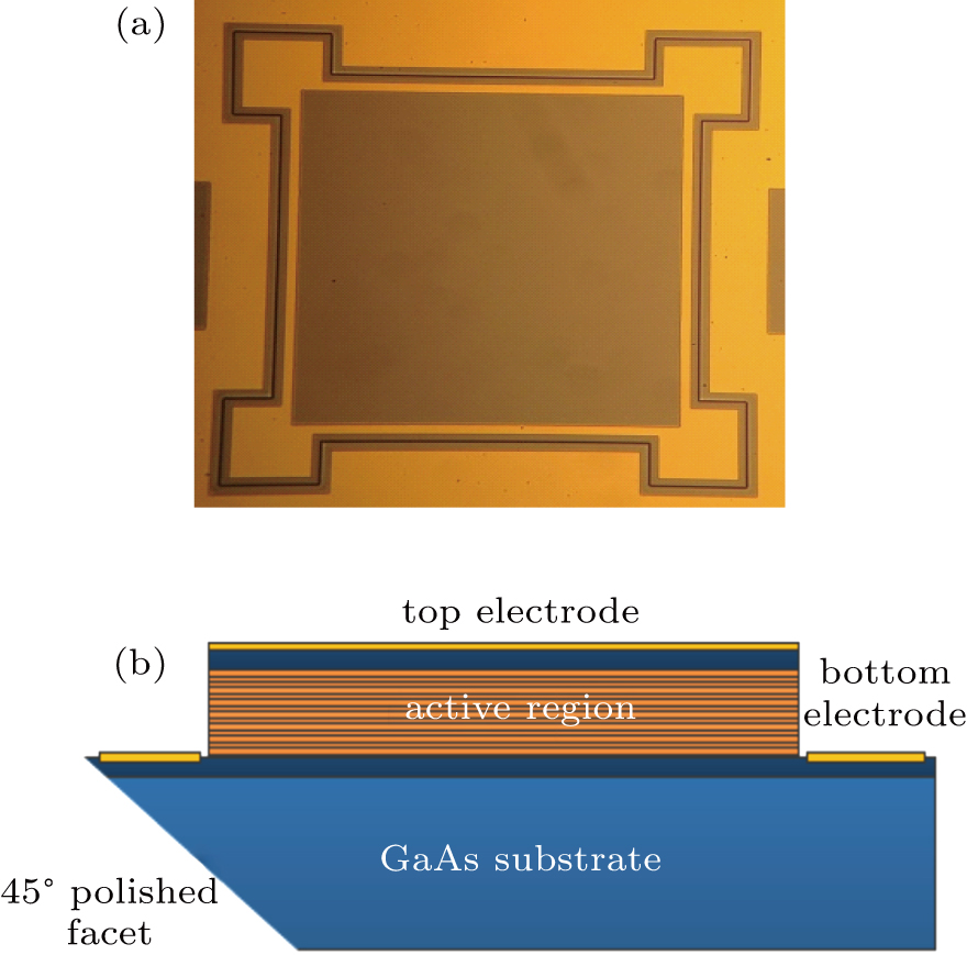
The device is fabricated using the standard GaAs semiconductor processing techniques. Firstly, we use the photolithography to define the mesa size. Then the ion-coupled-plasma etching is employed to etch the active region to form an square mesa. The etching depth is around . Then, the electron beam deposition, lift off, and thermal annealing techniques are used to fabricate the top and bottom metallic electrodes. Finally, to achieve the terahertz light coupling, we polish the GaAs substrate to complete the 45° facet geometry. Figure 1(a) is the optical image of a fabricated terahertz QWP mesa device. The four big metallic pads located at the corners of the square are prepared for wire bonding. Before the device characterization, we use the four-probe method to measure the resistance of the mesa device. The measured device resistance is 2Ω which indicates that we obtain good ohmic contacts. For the intersubband QWPs, the selection rule determines that only the light with an electric field component along the growth direction can be absorbed. Therefore, the wafer is finally processed into the 45° edge facet geometry as shown in Fig. 1(b).
Fig. 1. (color online) (a) Optical microscope image of a terahertz QWP mesa with a surface area of . (b) Schematic plot of the cross-section of a terahertz QWP with a 45° edge facet.
2.2. Characterization
To facilitate the device characterizations at different cryogenic temperatures, the cleaved QWP mesa is mounted onto a cold figure of a liquid helium cooled cryostat. Within the cryostat with a high density polyethylene (HDPE) window, the electrical and optical characteristics can be recorded. The dark current characteristics can be measured in voltage and current sweeping modes using a high-precision power source. The photocurrent spectra are measured using a Fourier transform infrared spectrometer (FTIR) equipped with a broadband Globar source. In this measurement, the cryostat is placed in the sample chamber of the FTIR and the QWP device is at the focal point of the external terahertz beam emitted from the Globar source. The photocurrent signal is sent back to the FTIR for generating the spectra. A low noise current amplifier (SR570) with an amplification ratio of 200 nA/V is used to amplify the photocurrent at different bias voltages. The responsivities of the detectors are measured by using a calibrated blackbody source with a temperature of 1000 K and a numerical aperture of 0.2 inch.[21] The noise spectral density is measured using a spectrum analyzer and then the noise equivalent power (NEP) is derived from the responsivity and the noise spectral density.
3. Results and discussion
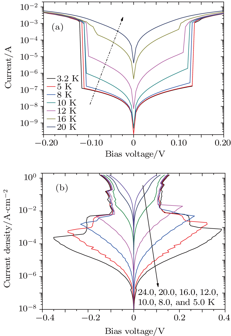
Figure 2 shows the dark current–voltage (I–V) characteristics of a terahertz QWP mesa () in voltage sweep mode (a) and current sweep mode (b) at different temperatures. Concerning the voltage sweeping measurement shown in Fig. 2(a), when the temperature is lower than 16 K, we can clearly see the current discontinuity (kink) in each curve. For example, at 5 K two kinks at the symmetric voltages of ±0.13 V are observed. The kink corresponds to the NDR region. As the temperature is increased, the current discontinuity happens at lower voltages, and when the temperature is higher than 16 K, the current discontinuity disappears. This phenomenon can be interpreted by quantum well impact ionization theory.[22] When the bias voltage is less than the jump voltage (at the current jump point), the multi-quantum wells structure is in a resistive “down” state that corresponds to the NDR region, which cannot be measured with the voltage-sweeping mode due to the multi-value behavior of NDR at a fixed bias voltage.[17]
Fig. 2. (color online) Dark I–V curves measured in (a) voltage sweep mode and (b) current sweep mode at different temperatures. The mesa size of the terahertz QWP is .
It is worth noting that the breakdown voltage of the device can be higher than the kink voltage. In order to determine the breakdown voltage and observe the NDR phenomenon, we measure the I–V curves in current-sweeping mode as shown in Fig. 2(b). In Ref. [17], we adopted a hot electron model to describe the NDR behavior at 5.0 K. In this paper, we mainly study the dependence of the NDR on the temperature experimentally. We can see that the NDR regimes appear in the voltage–current curves when . At T = 16 K, there is only a kink instead of an NDR regime, and the NDR behavior completely disappears at . As the temperature increases, the NDR regime starts at the point of lower bias voltage and higher current density, and the tested breakdown voltages at 5 K in the current-sweeping mode are ±0.35 V, which are two folds of the value obtained in the voltage-sweeping mode.
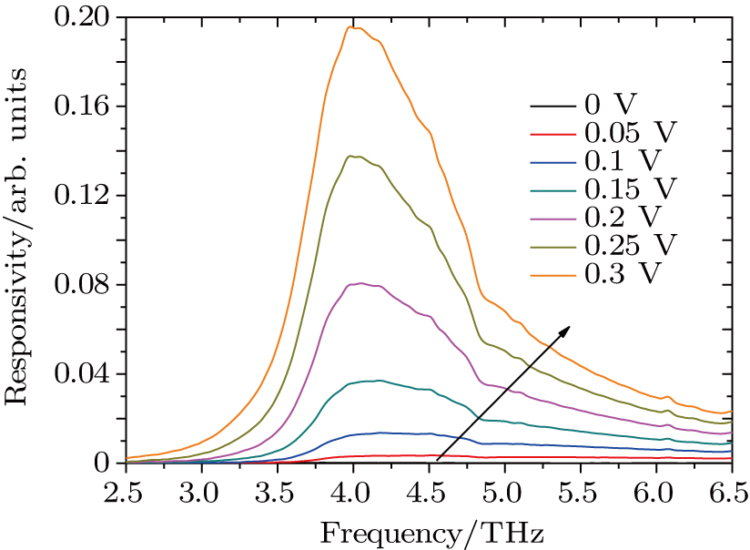
The experimental photocurrent spectra at 5.0 K are shown in Fig. 3. With the increase of the bias voltage from 0.05 V to 0.3 V, the peak responsivity increases monotonously, and the peak response frequency slightly shifts to the lower frequency (from 4.3 THz to 4.0 THz), which is resulted from the rise of the dark current. It can be seen from Fig. 3 that when the bias voltage increases from 0 V to 0.3 V, the device response is very stable, which indicates that the breakdown voltage agrees well with the observed voltage in the current sweep mode (Fig. 2(b)).
Fig. 3. (color online) Photocurrent spectra measured at 5.0 K with different bias voltages.
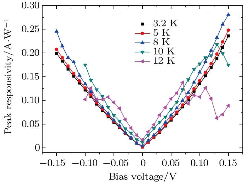
The peak responsivity as a function of the bias voltage at different temperatures is depicted in Fig. 4. As shown in Fig. 4, we obtain a relatively high responsivity of 0.3 A/W at the temperature of 8 K and the bias voltage of 0.15 V. The results show that the peak responsivity increases with the absolute value of the voltage.
Fig. 4. (color online) Peak responsivity versus bias voltage at different temperatures.
One of the most important characteristics of QWP devices is the detection sensitivity , which represents the signal (per unit incident power) to noise ratio appropriately normalized by the detector area and the measurement electrical bandwidth.[14] According to Ref. [14], can be calculated by
where R is the peak responsivity which can be extracted from the experimental data in Fig. 4, A is the length of a side of the mesa device, and is the device area. is the current noise power spectral density, where in is the noise current and Δ f is the the measurement bandwidth. The noise equivalent power (NEP) of the device can be expressed as
By combining Eqs. (1) and (2), the detection sensitivity can be calculated as
The NEP can be measured by a spectrum analyzer and a low noise current amplifier (SR570). Calculated by formula (3), the of our QWP device at 0.15 V is Jones (see Table 2). This relatively high value is comparable to some infrared detectors such as the commercial liquid helium cooled silicon bolometer.
Table 2.
Table 2.
Table 2.
Detection sensitivity of 4.3 THz QWP at different voltages.
.
Bias voltage/V
Peak responsivity/(A/W)
NEP/(pW/
Jones
−0.1
0.50
0.50
8
−0.05
0.22
1.08
3.70
0
0.008
30.26
0.132
0.05
0.24
1.03
3.88
0.1
0.56
0.44
9.09
0.15
0.99
0.26
15.4
Table 2.
Detection sensitivity of 4.3 THz QWP at different voltages.
.
4. Conclusion
We designed and fabricated a high performance GaAs/AlGaAs-based QWP device with a peak response frequency of 4.3 THz. We measured the dark current, the NDR phenomenon, and established the breakdown voltage at current-sweeping mode. The photocurrent spectrum and the blackbody response current spectrum of the device were also recorded. Based on the experimental results, we calculated the peak response rate to be about 0.3 A/W (at 0.15 V, 8 K), and the detection sensitivity was measured to be higher than 1011 Jones, which is comparable to the commercialized liquid helium cooled silicon bolometer.