† Corresponding author. E-mail:
InP-based high electron mobility transistors (HEMTs) will be affected by protons from different directions in space radiation applications. The proton irradiation effects on InAlAs/InGaAs hetero-junction structures of InP-based HEMTs are studied at incident angles ranging from 0 to 89.9° by SRIM software. With the increase of proton incident angle, the change trend of induced vacancy defects in the InAlAs/InGaAs hetero-junction region is consistent with the vacancy energy loss trend of incident protons. Namely, they both have shown an initial increase, followed by a decrease after incident angle has reached 30°. Besides, the average range and ultimate stopping positions of incident protons shift gradually from buffer layer to hetero-junction region, and then go up to gate metal. Finally, the electrical characteristics of InP-based HEMTs are investigated after proton irradiation at different incident angles by Sentaurus-TCAD. The induced vacancy defects are considered self-consistently through solving Poisson’s and current continuity equations. Consequently, the extrinsic transconductance, pinch-off voltage and channel current demonstrate the most serious degradation at the incident angle of 30°, which can be accounted for the most severe carrier sheet density reduction under this condition.
In recent years, space exploration activities have been conducted more and more frequently and in depth, which necessarily requires all kinds of semiconductor devices and relative integrated circuits to be used in electronic systems of spacecrafts.[1,2] Among them, InP-based high electron mobility transistors (HEMTs) demonstrate extremely excellent characteristics, such as high frequency, low noise figure, superior gain performance, and so on.[3–6] Consequently, they become significantly competitive candidates for various high-speed space applications, such as national defense, aerospace, and satellite radar.[7]
Semiconductor devices and their integrated circuits have been used in harsh space environments, and they are inevitably affected by various radiation particles and rays from different directions, such as protons, electrons, neutrons, γ rays, α rays, β rays, and other secondary atomic radioactive particles,[8–10] especially, protons and electrons, which are the most abundant particles in space radiation environment. Moreover, the mass of each proton is about 1836 times heavier than that of an electron, which means more serious irradiation damage of protons. Even if radiation dose of protons may be very low, the long-time accumulated irradiation will be bound to result in performance degradation of semiconductor devices and even failure of electronic systems.
Considering high technology maturity, low fabrication cost and broad applications, research about proton irradiation effect and hardness techniques chiefly focus on Si-based complementary metal-oxide-semiconductor transistor (CMOS) and silicon-on-insulator (SOI) devices.[11,12] Admittedly, some exploratory studies have been reported to aim at proton irradiation effect on various devices with III–V materials,[13,14] and the incident direction of proton particles is almost without exception perpendicular to the device surface for both simulations and experiments. However, few studies address the effects of proton irradiation from different orientations on InP-based HEMTs, which are in accordance with actual space radiation situation.
In this paper, the proton irradiation effect on InAlAs/InGaAs hetero-junction of InP-based HEMTs is investigated by SRIM software at a proton energy of 100 keV and incident angles in a range of 0°–89.9°. On this basis, the electrical characteristics and damage mechanism of InP-based HEMTs are also analyzed under proton irradiation at different incident angles. These studies will be helpful in improving the stabilities and durabilities of relative electronic systems.
The schematic cross-section of the InP-based HEMT is shown in Fig.
As is well known, carriers are usually gathered around InAlAs/InGaAs hetero-junction in InP-based HEMT, which thus determines almost all the device characteristics, including channel current, transconductance, frequency performances, etc. Therefore, the irradiation effect of InAlAs/InGaAs hetero-junction structure can provide a theoretical basis for damage mechanism of InP-based HEMTs and even radiation-hardened scheme. The hetero-junction structure is thus intercepted from actual device,[15] which includes Ti/Pt/Au gate metals, 15-nm-thick In0.52Al0.48As barrier and spacer layer, 15-nm-thick In0.53Ga0.47As channel layer and 500-nm-thick In0.52Al0.48As buffer layer as shown in Fig.
The damage mechanisms of proton irradiation on semiconductor devices mainly include ionization damage and displacement damage. Ionization damage mainly produces electron-hole pairs by breaking the energy band balance, and the number of the produced electron–hole pairs is proportional to the ionization energy loss (IEL) of incident protons. Displacement damage forms vacancies and replacement atoms by collision between protons and lattice atoms. Nevertheless, InP-based HEMTs have no semiconductor–insulator interfaces to capture free charges, therefore, the electron–hole pairs produced by ionization effect can be quickly recombined by diffusion motion and cannot have a permanent effect on the device characteristics. Namely, the degradation degree of device characteristics after proton irradiation is directly dependent on the number of induced vacancies by displacement effect.
The number of induced vacancy defects around InAlAs/InGaAs hetero-junction by each perpendicular incident proton is calculated by SRIM software with proton energies ranging from 40 keV to 170 keV as shown in Fig.
 | Fig. 3. (color online) Variation of induced vacancy with proton energy in InAlAs/InGaAs hetero-junction. |
As illustrated above, the damage degree of the device after proton irradiation is directly related to the number of induced vacancies by the displacement effect. The average number of vacancy defects generated in InAlAs/InGaAs hetero-junction by each proton is obtained by integrating the vacancy density curve with respect to distance as depicted in Fig.
 | Fig. 4. (color online) Variations of (a) the number of induced vacancy defects and (b)vacancy energy loss with incident angle of proton. |
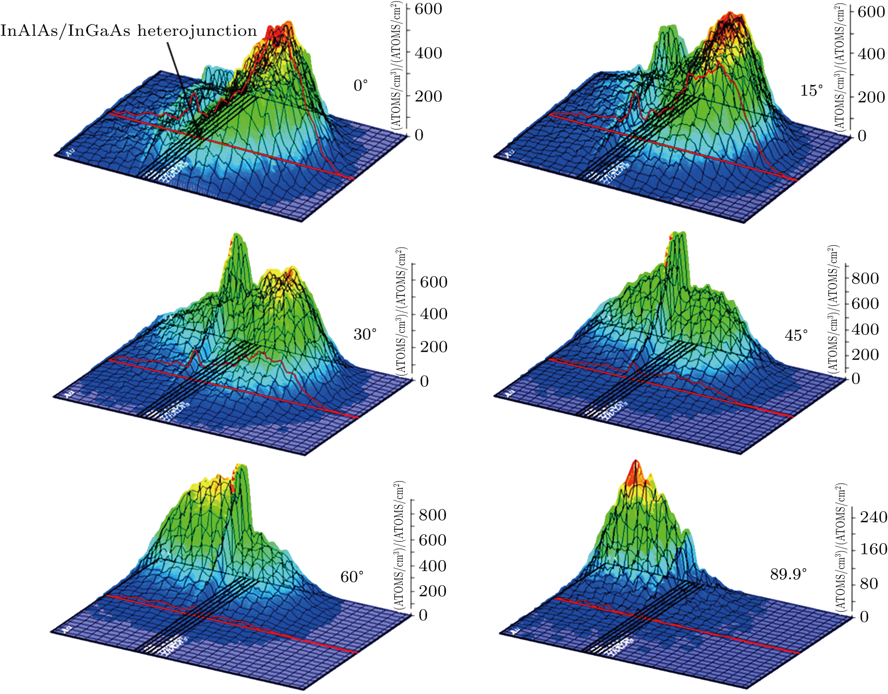
Actually, the damage degree of hetero-junction after proton irradiation from different directions can be intuitively reflected through distribution of incident protons, that is, the damage region. The average range and ultimate stopping positions of protons in target object at different incident angles at 100 keV are shown in Figs.
 | Fig. 5. (color online) Average range of protons in hetero-junction structure at different incident angles. |
As mentioned above, numerous vacancy defects are generated in InAlAs/InGaAs hetero-junction region by displacement effect after proton irradiation. The induced vacancies may influence device performances by acting as acceptor or donor defects, including As acceptor defects, In and Ga donor defects.[17] The acceptor-like defects of As vacancies behave as compensation centers of majority carriers, and thus result in performance degradation of InP-based HEMT. The induced As vacancy concentrations after proton irradiation are obtained from SRIM software at incident angles ranging from 0° to 89.9°, and the incident proton energy and fluence are set to be 100 keV and 2×1012 cm−2 in simulations. Successively, the influences of proton irradiation at different incident angles on electrical characteristics of InP-based HEMTs are investigated by Sentaurus-TCAD software. Reasonable physical models are used to describe the device performances, including hydrodynamic transport model, density gradient model, recombination models, etc. Moreover, the induced As vacancies were considered self-consistently through solving Poisson’s and current continuity equations.[18]
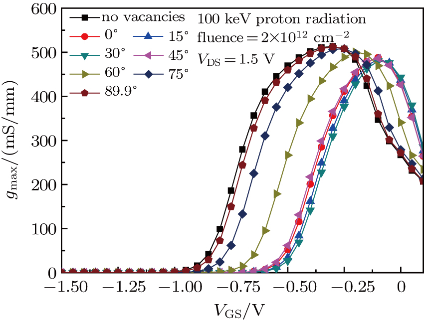
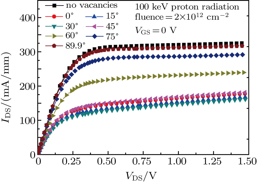
Figure 


 | Fig. 7. (color online) Plots of extrinsic transconductance versus gate-bias voltage of InP-based HEMTs after proton irradiation at different incident angles. |
 | Fig. 8. (color online) Plots of maximum extrinsic transconductance and pinch-off voltage of InP-based HEMTs after proton irradiation versus incident angle. |
 | Fig. 9. (color online) I–V characteristics of InP-based HEMTs after proton irradiation at different incident angles. |
The electron concentration in the channel region is investigated after proton irradiation at different incident angles, as shown in Fig.
The influences of proton irradiation from different orientations on InAlAs/InGaAs hetero-junction are studied with a proton energy of 100 keV. As the proton incident angle increases, the damage region moves gradually from buffer layer to hetero-junction region, and finally toward gate metal. Both the number of induced vacancy defects in InAlAs/InGaAs hetero-junction region and vacancy energy loss of incident protons increase slightly and then decrease sharply after the incident angle has reached 30°. Consequently, the extrinsic transconductance, pinch-off voltage and channel current demonstrate the most serious degradation at an incident angle of 30°, which can account for the most severe carrier sheet density reduction by the largest number of induced vacancy defects in InAlAs/InGaAs hetero-junction region. The above conclusions can provide a reliable theoretical guidance for assessing and reducing irradiation damage to InP-based HEMTs in space applications.
| [1] | |
| [2] | |
| [3] | |
| [4] | |
| [5] | |
| [6] | |
| [7] | |
| [8] | |
| [9] | |
| [10] | |
| [11] | |
| [12] | |
| [13] | |
| [14] | |
| [15] | |
| [16] | |
| [17] | |
| [18] | |
| [19] | |
| [20] |


