A transparent electromagnetic-shielding film based on one-dimensional metal–dielectric periodic structures
Zhao Ya-li1, 2, Ma Fu-hua2, Li Xu-feng3, Ma Jiang-jiang2, Jia Kun2, Wei Xue-hong1, †
College of Chemistry and Chemical Engineering, Shanxi University, Taiyuan 030006, China
Shanxi Key Laboratory of Electromagnetic Protection Technology, Taiyuan 030006, China
School of Applied Science, Taiyuan University of Science and Technology, Taiyuan 030024, China


† Corresponding author. E-mail: xhwei@sxu.edu.cn

Project supported by the International Science & Technology Cooperation Program of China (Grant No. 2014DFR10020) and the Science Foundation of Shanxi Province, China (Grant Nos. 201701D121050 and 201701D121007).

Abstract

In this study, we designed and fabricated optical materials consisting of alternating ITO and Ag layers. This approach is considered to be a promising way to obtain a light-weight, ultrathin and transparent shielding medium, which not only transmits visible light but also inhibits the transmission of microwaves, despite the fact that the total thickness of the Ag film is much larger than the skin depth in the visible range and less than that in the microwave region. Theoretical results suggest that a high dielectric/metal thickness ratio can enhance the broadband and improve the transmittance in the optical range. Accordingly, the central wavelength was found to be red-shifted with increasing dielectric/metal thickness ratio. A physical mechanism behind the controlling transmission of visible light is also proposed. Meanwhile, the electromagnetic shielding effectiveness of the prepared structures was found to exceed 40 dB in the range from 0.1 GHz to 18 GHz, even reaching up to 70 dB at 0.1 GHz, which is far higher than that of a single ITO film of the same thickness.

1. Introduction

Transparent shields (TS) have attracted great attention due to their promising applications, e.g., in personal electronic devices and the avionics aboard aircrafts and airplanes.[1,2] Such screens have been used as shields against electromagnetic interference (EMI) in the radio frequency range.[3,4] Yet it still remains difficult to achieve desirable results. For instance, metallic meshes may be bulky and heavy. In comparison, ITO films are relatively cheap and allow for a high transmittance in the visible range, but their shielding effectiveness (SE) against EMI is rather poor, which is 20 dB at 18 GHz.[5] At the same time, dielectric/metal/dielectric multilayers have also been extensively studied because they allow us to combine a high transparency with a good electrical conductivity. Such coatings have mainly been used for the fabrication of displays and solar energy control glasses.[68]

One-dimensional metal–dielectric photonic band gap (1D MD PBG) materials consisting of alternating metal and dielectric layers have been studied by a number of research groups.[914] The main characteristics of such structures are as follows: some wavelength ranges are mostly reflected, giving rise to the so-called band gaps, while other wavelength ranges are transmitted well due to the existence of pass bands.[15,16] Both the location and the width of the gap generally depend on the size of a unit, the index contrast, and the components’ thickness ratio.[17,18] It has been shown that the presence of a 1D MD PBG can enhance the total optical transmittance, and as a result, those structures have been described as “transparent metals”.[19] Meanwhile, it has been demonstrated that the total reflection can be improved by inserting metal layers into a general dielectric photonic crystal.[1416] Furthermore, it was reported that the SE of 1D MD PBG materials can exceed 40 dB in 30-kHz range to 1000-MHz range.[20] In this paper, we report an even better SE higher than 40 dB in the range from 0.1 GHz to 18 GHz, and it is able to reach values higher than 70 dB at 0.1 GHz. We hope to reveal the regulation mechanism for adjusting the optical performance and achieving a high SE of 1D MD PBG materials. So as to distinguish the difference between monolayer Ag film and the 1D MD PBG structure, the optical properties of monolayer Ag film was measured as well.

2. Fabrication and characterization of the 1D MD PBG structure

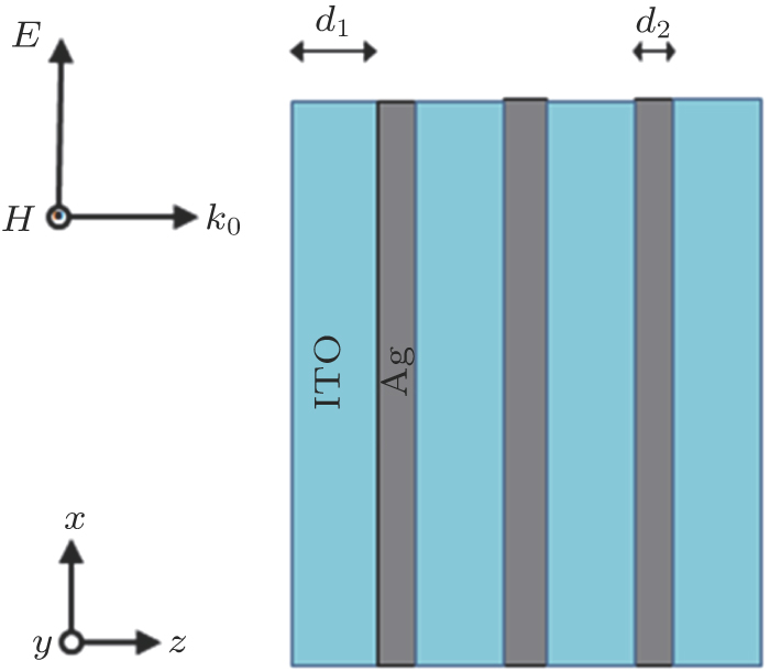
In this work, 1D MD PBG material consists of alternating ITO and Ag layers, with the structure being periodic in the z direction and uniform in the x and y directions, as shown in Fig. 1. A unit is composed by adjacent ITO and Ag layer. ITO film was made to be the topmost layer to protect the Ag from oxidation. Here η represents the film thickness ratio of each layer of the Ag film (d2) to the ITO film (d1), as given by Eq. (1).

Fig. 1. (color online) Structure of 1D MD PBG.

The films of ITO and Ag were sequentially deposited on glass substrates by magnetron sputtering. The system can automatically deposit 18 layers without destroying the vacuum. Prior to the deposition, the substrates were ultrasonically cleaned in acetone (CP). Then, the substrates were rinsed with deionized water (18 MΩ⋅cm) and baked at 300 °C in vacuum. The size of the substrate surface was 500 mm × 400 mm. Before sputtering, the substrates were transported from the loading chamber to the sputtering chamber via the substrate holder. Both the ITO target (10-wt.% SnO2-doped In2O3) and the Ag target (99.99% purity) had a surface area of 610 mm × 128 mm. The targets were fixed and the substrates were moved in front of the target during the sputtering process. The target-to-substrate distance was 140 mm. The ITO films were deposited at a power of 1500 W by DC magnetron sputtering and the Ag layers were sputtered at 350 W via radio frequency sputtering, respectively. During the deposition of the ITO films, the argon (99.995% purity) and oxygen (99.995% purity) flow rates were adjusted to 50 sccm and 1 sccm, respectively. In order to prevent an oxidation of the Ag films, the Ag films were deposited under argon atmosphere at a flow rate of 50 sccm. The base pressure was about 10−3 Pa and the working pressure was 0.67 Pa. The ITO and Ag growth rates were 2.5 nm/s and 2.0 nm/s, respectively. The growth rates were obtained by dividing the film thickness by the corresponding growth time, with the thickness measured using an ellipsometer (SENTECH SE8000dv-PV) and the growth time being controlled through the movement speed of the substrate holder. After fabricating the 1D MD PBG samples, the transmittance spectra of which in the UV-visible range from 300 nm to 800 nm were measured using a spectrophotometer (Shimadzu UV-310) with a resolution of 1nm. Furthermore, x-ray diffraction (XRD) measurements were carried out over the 2θ range from 10° to 70°, with a step size of 0.05° and a scanning speed of 3°⋅min−1, using a Bruker D8 x-ray diffractometer (theta-theta geometry). The surface morphology of 1D MD PBG samples was studied by scanning electron microscopy (SEM Hitachi SU3500). Accordingly, the SE was characterized utilizing the shielding chamber method with a screen size of 295 mm × 165 mm. SE of a medium is defined as follows: where A1 denotes the attenuation coefficient at a certain power when the characterized medium is not installed in the shielding chamber, which is composed of metal sheets, whereas A2 denotes the attenuation coefficient measured in the shielding chamber in the case that the characterized medium is installed. The difference between the measured and the standard value was found to be less than °4 dB. For the characterization process, a radio frequency (SMT02) and a microwave signal generator (SMR40) were used. Additionally, a spectrum analyzer (E4440A), a double cone, and a horn antenna (HK110, HL223, and HF906) were also used.

The optical performance was investigated by means of finite difference time domain (FDTD) simulation.[21] For the Ag films, the frequency dispersion of which was obtained via a modified Drude model as follows: where ε′ and ε″ represent the real and the imaginary part of the permittivity of the Ag films, respectively. The values for the plasmon frequency (ωp = 14.0 × 10¹⁵ rad/s) and the damping constant (Γ = 0.032 × 10¹⁵/s) were taken from the literature.[22] The empirical values of ε for silver are about 5 which is a sum or integral value after taking all pertinent transitions into account.[22] Additionally, the refractive index of ITO films was determined to be 1.7702 using a SENTECH SE8000dv-PV ellipsometer. In the visible wavelength range, the imaginary part of permittivity of the ITO film is so small that it can be ignored. For the simulations, the refractive index of the substrate was set to be approximately 1.52 for a wide optical range. The permeability of Ag and ITO films was treated as being constant (μ1 = μ2 = 1). The parameters used during the simulations for all samples are listed in Table 1.

Table 1.

Parameters of different samples.

.
3. Results and discussion
3.1. Sample structure and morphology

The SEM micrographs and XRD patterns obtained for the prepared 1D MD PBG structure consisting of 3.5 periods of Ag and ITO (sample #4) are shown in Fig. 2. As is shown in the figure, the surfaces of Ag and ITO films are smooth and the grains are relatively compact and small. In our work, the size of Ag particles was typically larger than 100 nm due to thermal diffusion when the deposition temperature was higher than 100 °C for the same structure with sample #4. This is why the sample was not deliberately heated during the deposition process. The size of Ag grains in sample #4 is about 20 nm to 50 nm, which is clearly larger than that of ITO grains. This difference should be due to three dimensional growth mode of the Ag grains.[23] The observed diffraction peaks in the XRD pattern correspond to the (211), (222), (400), (411), (440), (611), and (622) planes of the ITO phase. The Ag diffraction peak was broad and weak. Both the films of Ag and ITO showed a crystalline structure.

Fig. 2. SEM images of Ag films (a) and ITO films included in #4 sample and XRD (c) corresponding to sample 4.
3.2. Optical characterization

Next, the optical characteristics of the Ag films and the 1D MD PBG structure were investigated. The experimentally obtained optical transmittances of the Ag films with the thicknesses of 5 nm, 14 nm, and 22 nm are presented in Fig. 3. Obviously, the transmittance is approaching zero below 320 nm for band-to-band transition. It suddenly reaches its maximum at nearly 320 nm and then dramatically decreases. The thicker the Ag films, the faster the drop of the transmission line with increasing wavelength. One can see clearly the transparent range is hardly adjusted.
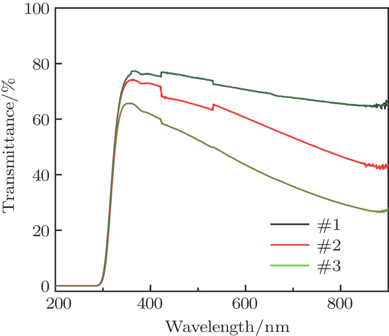
Fig. 3. (color online) The transmission of monolayer Ag films with thickness 5 (#1), 14 (#2), and 22 nm (#3), respectively.

The transmission was simulated by FDTD in the range from 400 nm to 800 nm for 1D MD PBG structure consisting of 3.5 periods. Keeping the thickness of the Ag films at 20 nm, the thickness of each of the ITO layers was varied from 10 nm to 100 nm and thus η was changed from 1:5 to 2:1. As shown in Fig. 4, the central wavelength of the transmission spectrum red-shifts with η decreasing. In order to further demonstrate the influence of η on the optical performance, the transmissions of multiple samples were simulated for η fixed at 1:1, 1:2, 1:3, and 1:4, respectively, which corresponds to central wavelengths of lower 400 nm, 410 nm, 475 nm, and 510 nm. The width of the transmission peak remarkably broadened with the ITO film thickness increasing. However, compared to the simulated transmittance of 1D MD PBG sample containing the 40-nm ITO films which is not given in the paper, it was found that, once the thickness of the ITO layers exceeds 60 nm, two transmission peaks appear, which is in good agreement with previous results and is due to the traveling wave interference across the multilayers structure.[24,25] The maximum transmission can nearly reach up to 100% due to the enhancement of the transmission caused by the strong coupling between the waveguide mode and the surface plasmon, when 1D MD PBG structure behaves as a waveguide.[26]

Fig. 4. (color online) Optical transmittance spectra of 1D MD PBG as a function of d1 when d2 = 20 nm (a), transmission spectra of cases for d1 = 20 nm, 40 nm, 60 nm, and 80 nm when maintain d2 being 20 nm (b).

To further investigate the effect of η on the optical performance of 1D MD PBG structure, the thickness of the Ag layers was varied from 10 nm to 15 nm to 20 nm, while the thickness of the ITO layers was fixed at 60 nm, again with 3.5 pairs. Here, η is equal to 1:2, 1:3, and 1:4, respectively. Compared to Fig. 4, the second peak has clearly disappeared and there is only one peak in Fig. 5. This further suggests that the existence of two peaks is due to the thicker ITO films. A similar regulation mechanism was found, i.e., a redshift of the central wavelength and a widening of the spectrum with η decreasing. Moreover, the transmittance was found to increase with η decreasing, and the transmittance can reach more than 98% despite the fact that the total thickness of the Ag film is much thicker than the skin depth (5 nm to 6 nm) in the optical range.
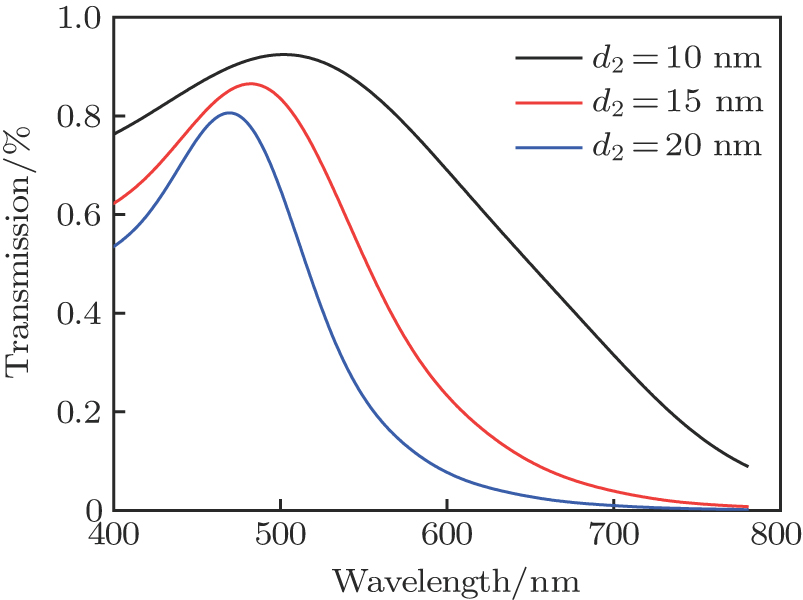
Fig. 5. (color online) Optical transmittance spectra of 1D MD PBG as function of d2 when d1 = 60 nm.

When comparing the experimental and simulation results obtained for sample #4, one can clearly see that the measured central wavelength is in good agreement with the theoretical results, as shown in Fig. 6(a). However, the experimental optical transmission intensity is far lower than that of the intensity simulated by FDTD. This may be attributed to two reasons. First, there may be a larger surface plasmon resonance absorption induced by the rough Ag film. Second, the small thickness of the Ag film might have induced a higher optical absorption. During FDTD simulation, the frequency dispersion of Ag was obtained through a modified Drude model (Eq. (2)), in which the damping parameter Γ is considered to be constant. However, in practice, Γ is not a constant but obviously increases when the thickness of the metal film is lower than a few tens of nanometers.[22] In the optical range, the value of ω is far larger than that of Γ. Thus, according to Eq. (4), the imaginary part of ε′ is proportional to Γ

Fig. 6. (color online) Experimental and simulated optical transmittance spectra of #4 (a), and optical transmittance spectra of #4, #5, and #6 (b).

The fixed value of Γ, however, is no longer valid when the thickness of the metal film is below a few tens of nanometers. Γ is a collision rate related to the electron mean free path l in the metal. For a metal nanostructure, the effective mean free path l1 is reduced according to the following Eq. (5)[22] Here, R represents the thickness of the metal films. Then the nanostructure damping parameter Γ1 that considers the size effect can be written as where a is of the order of one and depends on the specific geometry and some other factors, and vF is the Fermi velocity. According to Eq. (4), therefore, because Γ1 is much larger than Γ as indicated in Eq. (6), the magnitude of ε″ is substantially larger than the corresponding bulk value when the thickness of the metal film is of the order of tens of nanometers or smaller. Larger losses will be induced due to the larger magnitude of ε″. However, the magnitude of ε′ only slightly differs from the value for the bulk metal because the real part of the dielectric function ε′ is only marginally related to the damping constant. Thus, the central wavelength slightly changes, whereas the transmission intensity drastically decreases. Samples #4, #5, and #6 correspond to 3.5, 4.5, and 5.5 periods of the prepared 1D MD PBG structure with an η of 1/4, as shown in Fig. 6(b). The measured central wavelength corresponds to 496 nm, 502 nm, and 530 nm, respectively, and the transmission width slightly broadens. Interestingly, the transmittance of the 1D MD PBG structure increases and then decreases with the number of periods, as shown in Fig. 6(b).

3.3. Shielding effectiveness

In a study based on the experiment, the period of 1D MD PBG structure is 3.5 by selecting when sufficient shielding effect has been obtained.[27] In order to obtain a high SE, the influence of η on the SE was also investigated. The experimental data are shown in Fig. 7. The thickness of the ITO films was maintained at 40 nm, while η was varied from 1/4 to 1/3 and 1/2, respectively. The SE can obviously be increased at each frequency by increasing the value of η, as illustrated in Fig. 7. Most notably, SE could be improved from 40 dB to 65 dB at 3 GHz by increasing the value of η. It is a remarkable fact that the SE can reach values higher than 40 dB in the range from 0.03 GHz to 18 GHz and even reach 70 dB at 0.1 GHz when η is equal to 1:2. Commonly, in order to obtain a good SE, the thickness of the shielding medium must exceed the skin depth.[28] However, in our work, a perfect SE was obtained despite the fact that the total metal thickness was only several hundred nanometers, which is far thinner than the skin depth in the microwave range. We also investigated SE of a 1D MD PBG structure consisting of a 20-nm Ag film and found that the SE was not enhanced but instead decreased when the thickness of the ITO films was increased. Apparently, a high metal proportion is beneficial for improving SE. The phenomenon is due to the fact that the sign of εx or εy is opposite to that of the air permittivity at radio frequency. Here, εx and εy denote the effective permittivity in the directions that are parallel to 1D MD PBG structure. A larger η is associated with a larger absolute value of negative εx and εy. Then SE is enhanced with the increasing η.

Fig. 7. (color online) SE of samples with d1 = 1/4, 1/3, and 1/2 when maintaining d1

Compared to single ITO films of the same thickness, which are extensively used as transparent shields, the SE can be significantly improved over a wide frequency range from 0.03 GHz to 18 GHz when using the proposed 1D MD PBG structure, as shown in Fig. 8. For instance, SE can be improved to 50 dB from 20 dB at 1.5 GHz. Clearly, the fabricating 1D MD PBG structures is a very promising approach to obtain a light-weight and ultrathin shielding medium. As previously reported, better shielding or reflection performances can be achieved by inserting a very thin metal layer between two ITO films.[20] The very thin metal layer can reduce the coating sheet resistance by short-circuiting.

Fig. 8. (color online) SE of ID-PBG (#8) and ITO films (#7) with thickness of 300 nm.
3.4. Mechanism for tuning the optical performance

In this section, the mechanism for adjusting the optical performance will be discussed. When the thickness of each layer is sufficiently thinner than the incident wavelength, the 1D MD PBG structure can be described as homogeneous and having isotropic permittivity and permeability parameters. The whole system then could be treated as a single anisotropic medium with the permeability being equal to one and a permittivity as described below.[29,30] The permittivity of the ITO and the Ag films is defined as εd and εm, respectively, and can be calculated as follows: where x and y represent the directions parallel to the one-dimensional photonic crystal, respectively, and z represents the direction perpendicular to the surface of the photonic crystal. According to Eqs. (7a) and (7b), εx and εz were calculated, as shown in Fig. 9, where the sign of εz is always positive in the range from 400 nm to 800 nm, whereas the value of εx significantly decreases with increasing wavelength, and the sign becomes negative at a certain wavelength (450 nm when η is 1:2). As is well known, a positive value of εx is necessary for achieving a higher transmittance, and the optical reflectivity becomes larger and optical transmission will be inhibited for negative values of εx. Then, the transmission bandwidth, corresponding to the optical range with positive εx, as indicated by the gray section in Fig. 9, will become broader. The optical performance can be regulated by varying the structure analogously to FDTD simulations. When εx is equal to 1, the transmittance likely attains its maximum because of the low reflectivity, which is caused by impedance matching. Therefore, the wavelength corresponding to the maximum transmittance was determined to be 434 nm and 476 nm for η of 1:3 and 1:4, respectively, as shown in Fig. 9. Correspondingly, as shown in Fig. 5, the central wavelength simulated by FDTD was 469 nm and 482 nm, respectively. The difference between the theoretical and simulated results is acceptable.

Fig. 9. (color online) Real and imaginary parts of the effective permittivity for thickness ratios of 1:1, 1:2, 1:3, and 1:4.

Additionally, when the incident light wave reaches 1D MD PBG structure, the energy flow vector S0 no longer has the same direction as the phase vector k0, and the angle between them is denoted by α. As a result, the energy flowing in the z direction is a function of cos α, as shown in Eq. (8).[31] Here, n and c denote the medium’s refractive index and the speed of light in vacuum, respectively.

Generally, the angle between S0 and k0 is equal to that between the displacement vector D and the field vector E, as shown in Fig. 10. It can clearly be seen from Eq. (8) that the energy flowing in the z direction decreases as α increases.

Fig. 10. Relationship of E, D, S0, and k0.

According to Eq. (9), if the signs of εx, εy, and εz are all positive, α increases along with the absolute value of εxεz. However, as shown in Fig. 9, the absolute value of εxεz obviously decreases with η increasing.

This is why a smaller value of η promotes a higher optical transmission. The results generally are in good agreement with FDTD simulation results shown in Fig. 5.

4. Conclusions

In summary, we have designed and fabricated 1D MD PBG structures with various ITO to Ag film thickness ratios. The theoretical and simulated results suggested that a high thickness ratio of the dielectric layers contributes to the enhancement of the transparency in the visible region. The transmission band will slightly shift and broaden when gradually increasing the thickness ratio of the dielectric layers. The described mechanism clearly revealed that the transmission magnitude is determined by the angle between the energy flow vector S0 and the phase vector k0, which is determined by the absolute value of εxεz. Moreover, the absolute value of εxεz decreases as the thickness ratio of the metal/dielectric layers increases. The optical transparent band is determined by the bandwidth of the wavelength with positive εx. The central wavelength corresponds to the wavelength with εx = 1. Therefore, the optical transmission spectrum can be adjusted by varying εx. The central wavelength obtained through theoretical calculations, experiment, and FDTD simulations are all in good agreement. In addition, we observed that, when the thickness of ITO films is larger than 60 nm, there are two peaks in the transmission spectrum. Noticeably, SE was found to increase with the thickness ratio of the Ag films, and it can exceed 40 dB in the range from 0.1 GHz to 18 GHz and even reach 70 dB at 0.1 GHz. We also demonstrated that SE of the prepared 1D MD PBG structure is far superior to that of traditional ITO films. Thus, the 1D MD PBG structure is a good approach to obtain an ultrathin and light-weight electromagnetic shielding medium. The good invisibility performance in microwave range associated with a good transmittance in visible range indicates a high application potential of the prepared structures.

Reference
[1] Rivera D S Schulz J T Zuber V Turner R 2015 Magn. Reson. Mater. Phys., Biol. Med. 28 49
[2] Han J Wang X Qiu Y Zhu J Hu P 2015 Carbon 87 206
[3] Kim D Kim Y Kim J 2016 Mater. Des. 89 703
[4] Kumar P Reddy P V Choudhury B Chowdhury P Barshili H C 2016 Thin Solid Films 612 350
[5] Greco S Sarto M S Tamburrano A 2008 Symposium on Electromagnetic Compatibility 32 18
[6] Shih W C Kao K S Cheng D L Chung C J Hsieh P T 2013 Surf. Coat. Technol. 219 139
[7] Travkin V V Luk’yanov A Drozdov M N Vopilkin E A Yunin P A Pakhomov G L 2016 Appl. Surf. Sci. 390 703
[8] Yu S Li L Xu D Dong H 2014 Thin Solid Films 562 501
[9] Shen H Z Wang Z H Wu Y X Yang B 2016 RSC Adv. 6 4505
[10] Moslemi F Jamshidi-Ghaleh K 2016 J. Appl. Phys. 119 093101
[11] Xiao X Wenjun W Li S Zheng W Zhang D Du Q Gao X Zhang B 2016 Optik 127 135
[12] Yu W Jia X Long Y Shen L Liu Y Guo W 2015 ACS Appl. Mater. 7 9920
[13] Pavlichenko I Broda E Fukuda Y Szendrei K Hatz A K Scarpa G Lugli P Bräuchle C Lotsch B V 2015 Materials Horizons 2 299
[14] Mandal S Bose C Bose M K 2016 Opt. Quantum Electron. 48 200
[15] Xiao X Chen R 2015 Nano 10 1550088
[16] Luo Z Chen M Deng J Chen Y Liu J 2016 Optik 127 259
[17] Jena S 2016 Thin Solid Films 599 133
[18] Pradhan S K 2014 Opt. Express 24 12486
[19] Scalora M Bloemer M J Pethel A S Dowlin J P Bowden C M Manka A S 1998 J. Appl. Phys. 83 2377
[20] Sibilia C Bertolotti M 2003 Trans. Electromag. Compat. 45 586
[21] Oskooi A F Roundy D Ibanescu M Bermel P Joannopoulos J D Johnson S G 2010 MEEP: Comput. Phys. Commun. 181 687
[22] Cai W S Shalacv V 2010 Optical Metamaterials Berlin Springer 32
[23] Henry C R 1998 Surf. Sci. Rep. 31 231
[24] Pradhan S K Xiao B Skuza J R Santiago S K Mundle R Pradhan A K 2014 Opt. Expreess 24 12486
[25] Fan S Villeneuve P R Joannopoulos J D 1996 Phys. Rev. 54 11245
[26] Ebbesen T W Lezec H J Ghaemi H F 1998 Nature 391 667
[27] Zhao Y L Li K X Li X F et al. 2015 Acta Opt. Sin. 35 375 in Chinese
[28] Amore D Sarto M S Tamburrano A 2005 International Symposium on Electromagnetic Compatibility 3 900
[29] Wood B Pendry J B 2006 Phys. Rev. 74 115116
[30] Belov P A Hao Y 2006 Phys. Rev. 73 113110
[31] Markos P Soukoulis C M 2008 Wave propagation: from electrons to photonic crystals and left-handed materials Princeton Princeton University Press 56