Highly stable two-dimensional graphene oxide: Electronic properties of its periodic structure and optical properties of its nanostructures
Zhang Qin1, Zhang Hong1, 2, †, Cheng Xin-Lu2
College of Physical Science and Technology, Sichuan University, Chengdu 610065, China
Key Laboratory of High Energy Density Physics and Technology of Ministry of Education, Sichuan University, Chengdu 610065, China


† Corresponding author. E-mail: hongzhang@scu.edu.cn

Project supported by the National Key Research and Development Program of China (Grant No. 2017YFA0303600) and the National Natural Science Foundation of China (Grant Nos. 11474207 and 11374217).

Abstract

According to first principle simulations, we theoretically predict a type of stable single-layer graphene oxide (C2O). Using density functional theory (DFT), C2O is found to be a direct gap semiconductor. In addition, we obtain the absorption spectra of the periodic structure of C2O, which show optical anisotropy. To study the optical properties of C2O nanostructures, time-dependent density functional theory (TDDFT) is used. The C2O nanostructure has a strong absorption near 7 eV when the incident light polarizes along the armchair-edge. Besides, we find that the optical properties can be controlled by the edge configuration and the size of the C2O nanostructure. With the elongation strain increasing, the range of light absorption becomes wider and there is a red shift of absorption spectrum.

1. Introduction

During the past few decades, surface plasmons (SPs) in nanostructures have attracted a great deal of attention in nanoscience field, because they have remarkable effects on molecular spectroscopy,[1,2] optical waveguides,[3] optoelectronic devices,[4] bio-medical treatments,[5] etc. The SPs are of the harmonic oscillations of free electrons in metal nanostructures. The resonance frequency of SPs is affected by the factors of size,[6,7] shape,[8] and surrounding environment.[9] Usually, to excite plasmon, we mainly use traditional metal nanomaterials such as nanoparticles of gold, silver, copper, etc. However, there is a huge problem that the surface plasmons of the optoelectronic device of precious metal decay quickly in the propagation process. Moreover, the plasmonic device of precious metal has a relatively single performance of resonance mode, which cannot meet the requirements for the diversification of modern electronic devices. To overcome the difficulty, scientists have made great efforts for a long time and found that the metal-free materials can offset the insufficiency, and graphene is the most representative material.

Graphene is one of the most promising two-dimensional (2D) materials, which is structured by a planar honeycomb monolayer of carbon atoms.[10] It permits electrons to flow freely across its surface with particularly low scattering due to its electronic structure-Dirac cone.[11] In the applications of plasmon excitation, graphene has three advantages over precious metals: firstly, π plasmon has a long-range charge transfer excitation; secondly, electrons do not easily decay on the surface of graphene; thirdly, graphene has several vibration modes of energy. Due to the excellent properties of graphene, scientists have also done a lot of research on graphene derivatives, such as the substitutional doping of carbon atoms in graphene with transition metals (TMs) can tune the electronic and magnetic properties of graphene.[12] Moreover, van der Waals heterostructure of graphene and g-GaN can tune the Schottky barrier.[13] In addition, graphene oxide (GO) is also a prominent material of graphene derivatives. A lot of experiments have shown that GO has some superior properties compared with graphene, such as its excellent surface activity,[14] which can be eliminated by small molecules or polymers.[15] Besides, GO has an important status in 2D material for improving the thermal, electrical and mechanical properties.[1618] Current research on GO is not systematic nor comprehensive, therefore, it is necessary to do more research on GO.

In this paper, we theoretically predict a stable single-layer structure of graphene oxide (C2O). There are two oxygen atoms and four carbon atoms in the primitive cell. We use the first principles theory to study the stability and the electron structure of C2O. Through the calculations of the cohesive energy, formation energy and phonon spectrum of C2O, we obtain that the structure of C2O is stable. In addition, this type of C2O is a direct gap semiconductor from analyzing the electronic band structures and density of states (DOS). To study the optical properties of C2O nanostructures, TDDFT is used. By analyzing the structure of this type of C2O, we find that the structure of C2O is anisotropic when the light polarizes along different directions, which means that the C2O is a promising candidate of photoelectric switch. We focus on studying the optical properties of C2O nanostructures when the light polarizes along the armchair-edge direction. We consider the influence on the optical response by changing the edge configuration and size of the C2O nanostructure. What is more, the influence of changing the elongation strain has also been considered.[19] These studies will provide some theoretical support for the practical application of the optoelectronic devices which are made from C2O nanostructure. The rest of the paper is organized as follows. In Section 2, we present the computational methods. In Section 3, we show the stability and electronic structure of the single-layer C2O, and the optical response of the C2O nanostructures. Finally, some conclusions are drawn from the present study in Section 4.

2. Computational methods

All of our calculations were based on first-principle simulations. To study the stability, electronic band structure, density of states, and optical properties of single layer C2O, DFT was used in the generalized gradient approximation (GGA), which is expressed by the Perdew–Burke–Ernzerhof (PBE) functional.[20] The CASTEP[21] package was used with norm-conserving pseudopotentials and a plane-wave cutoff energy of 830 eV. Our structure model was fully relaxed, until the forces were less than 0.01 eV/Å and the energy tolerances were less than 5 × 10⁻⁶ eV per atom. A vacuum spacing between the 2D single-layer structures was 20 Å. We adopted the Monkhorst–Pack scheme for k-point sampling of the Brillouin zone with 21 × 21 × 1 for C2O. The phonon dispersion of C2O was calculated by the linear response method.[22] The calculations of the optical properties of C2O nanostructures were performed by the real-space TDDFT code OCTOPUS.[23] We described the oxygen atoms, carbon atoms and hydrogen atoms by the Troullier–Martins pseudopotential.[24] The GGA and PBE functional for the exchange–correlation potential were used in both the ground-state and the excited-state calculations, respectively. The excitation spectra induced by an impulse excitation were extracted by the Fourier transform of dipole strength. We defined the simulation zone by assigning a 6-Å-radius sphere around each atom and a uniform mesh grid of 0.2 Å. In the real-time propagation, Kohn–Sham wave function is evolved for 6000 steps in time steps of Δt = 0.003 eV−1.

3. Results and discussion
3.1. Stability and electronic structure of single-layer C2O

The crystal structure of C2O is given in Fig. 1. The number of the outermost electrons of carbon atoms is four and the number of oxygen atoms is six. It is possible to form a layered structure such as C2O of this type. The space group of C2O is PMMM (No. 47). The structural parameters of the optimized geometric C2O include lattice constants, bond length, layer height, and bond angle. The results of the optimized C2O structure are summarized in Table 1. To illustrate the stability of C2O, we conduct the cohesive-energy calculation and formation-energy calculation of C2O. In addition, we also carry out the phonon-dispersion calculation of C2O. The cohesive-energy Ecoh of C2O can be estimated from the following expression: where Etot represents the total energy of C2O, and Eatom is the energy of a free atom in the ground state. We calculate Eatom by placing each isolated atom in a cell with a cubic lattice of 10 Å to prevent the interactions between neighboring atoms. By calculating, we obtain that the cohesive energy of C2O is −7.83 eV/atom. However, we find that the thermal energy of C2O is lower than the cohesive energy at room temperature. To provide the conditions for synthesis of C2O, the formation energy of C2O is studied. The formation energy per atom (Eform) of C2O is evaluated by using the standard expression as follows: Similarly, Etot is the total energy of C2O, Emolecule (O2) is the energy of the oxygen molecule in the ground state. We calculate Emolecule by each isolated O2 molecule that is placed in a cell with a cubic lattice of 10 Å, which avoids the interactions between neighboring molecules. The E (graphene) is the total energy of single-layer graphene primitive cell. The formation energy of C2O is −0.21 eV/atom, which illustrates that the process of synthesizing C2O is an exothermic reaction, and the reaction can take place spontaneously. Therefore, we may synthesize C2O experimentally.[25]

Fig. 1. (color online) (a) Top view of C2O, (b) side view of C2O. Red spheres represent oxide atoms and grey spheres refer to carbon atoms, (c) Brillouin zone of C2O, (d) phonon band dispersion of C2O, from which we can find that the structure shows kinetic stability.
Table 1.

Results for optimized geometries of C2O, obtained by using DFT with the PBE exchange–correlation functional.

.

In addition, we perform the phonon-dispersion calculation of C2O. As shown in Fig. 1(d), the result of phonon is obtained from calculation along the high symmetric points in the Brillouin zone. We find that the phonon dispersion has no negative frequency, so it illustrates that this type of C2O is kinetically stable.[26]

Furthermore, we calculate the electronic band structure and density of states (DOS) of C2O, through using both PBE and the screened hybrid functional of Heyd–Scuseria–Ernzerhof (HSE06). As shown in Fig. 2(a), the valence-band maximum and the conduction-band minimum are near Y point, and the difference between these two energies is 1.231 eV which means that C2O is a direct gap semiconductor. Besides, to understand the contributions of different orbitals to the electronic states, we figure out the DOS and the partial densities of states (PDOSs) for C2O. The result is shown in Fig. 2(b). It is observed from the PDOSs of C2O that the states near the Fermi level (in green dashed frame) have contributions from the p orbitals of O, C1, and C2 (shown in Fig. 1(a)). In addition, at conduction-band minimum near 4.5 eV (in blue dashed frame), the contributions are mainly from p orbitals of O and C2. At valence-band maximum near −2.5 eV (in the area of red dashed frame), the contributions are from p orbitals of O and C2. Moreover, there is a large number of electrons at 4.5 eV and −2.5 eV, which may lead to a phenomenon that the absorption spectrum would have a very strong absorption peak near 7 eV.

Fig. 2. (color online) (a) Electronic band structures of C2O. Dotted line represents Fermi level. (b) Density of states (DOS) and the partial densities of states (PDOSs) of C2O. There are two identical O atoms, two identical C1 atoms, and two identical C2 atoms in the primitive cell of C2O, and O atom, C1 atom, C2 atom are shown in PDOSs, Fermi level is indicated by the dashed line.
3.2. Optical response of C2O nanostructure

We investigate the periodic structure of C2O. As shown in Fig. 3(a), we find that the light absorption spectra of C2O periodic structure ranges from visible region to near-ultraviolet region. Besides, we find that the periodic structure of C2O is anisotropic when we compare the two spectra in different directions of the incident light. The first absorption peak is at 3.39 eV, and there are two main absorption peaks at 4.89 eV and 6.42 eV, respectively, when the light polarizes along the armchair-edge. Moreover, the first absorption peak is at 3.21 eV, and there is a strong absorption peak at 7.48 eV when the light polarizes along the zigzag-edge.

Fig. 3. (color online) (a) Absorption spectra of (a) periodic structure of C2O and (b) 4 × 5 C2O rectangular nanostructure. X represents that the incident light polarizes along the armchair-edge. Y refers to the incident light that polarizes along the zigzag-edge.

Many experiments show that materials will have many unique properties, such as surface effect, quantum effect, and volume effect, when the macroscopic material is processed into the nanometer size. These small-scale nanostructures can be used in the fields of biological plasmon imaging, medical treatment, and quantum plasmon transfer. Moreover, in the practical application, the optoelectronic devices need higher and higher integration level and the sizes of primary elements need to be processed to be smaller and smaller until they can be processed into nanoscale. However, as is well known, because of the quantum confinement effect,[27] the optical properties of nanostructure material would have a considerable difference compared with those of macroscopic material. Therefore, in the rest of the paper, we focus on studying the optical properties of C2O nanostructures.

We use Cartesian coordinates and fix atoms in the XY plane, to deal with the rectangular C2O nanostructures that the armchair-edge is parallel to the X-axis direction, and the zigzag-edge is perpendicular to the X-axis direction. In addition, at the edge of rectangular C2O nanostructures, the dangling σ bonds at the edges are passivated by hydrogen atoms. Here, we regard the carbon ring (including oxygen atoms) as a basic unit, then the rectangular C2O nanostructures with different sizes are named X × Y, where X represents the number of basic units in the X-axis direction, Y refers to the number of basic units in the Y-axis direction.

Figure 3(b) shows the absorption spectra of 4×5 rectangular C2O nanostructure, when the incident light polarizes along different directions. There appear different absorption spectra in Fig. 3(b), we find that they show optical anisotropy. By comparison with the absorption spectra of the periodic structure of C2O, we find that there are some differences. The most prominent phenomenon is that the main peak is blue shifted. We analyze this case and draw a conclusion that with the decrease of the structure size, the quantum size effect exerts an influence on energy band structure, making the energy gap become wider, and resulting in the increasing of photonic band gap.

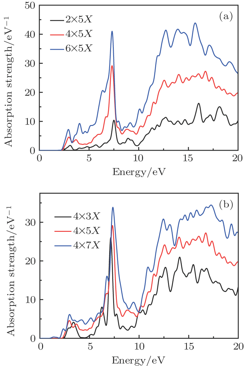
To study the effects of the size and the edge configuration of rectangular C2O nanostructures on their optical properties. We study the 2 × 5, 4 × 5, 6 × 5, 4 × 3, 4 × 7 rectangular C2O nanostructures, which are shown in Fig. 4. Because C2O nanostructures are optically anisotropic, and the light absorption is stronger when the incident light polarizes along the armchair-edge direction. We mainly study the optical properties of C2O nanostructures when the incident light polarizes along the armchair-edge. As shown in Fig. 5, we find that the nanostructures of C2O has light spectra with absorption from visible region to near-ultraviolet region. Because of the barrier of oxygen atoms, there is no main absorption peak in the low-energy resonance zone. In the structure of C2O, the electrons of oxygen atom are difficult to jump into adjacent C2 atom, because this process needs to overcome a great energy barrier, which may result from the fact that the rectangular C2O nanostructure has a main absorption peak near 7 eV. In addition, we show the absorption spectra of 2 × 5, 4 × 5, 6 × 5 rectangular C2O nanostructures in Fig. 5(a), where the incident light polarizes along the armchair-edge. We maintain the length along the zigzag-edge direction of rectangular C2O nanostructures to be unchanged, while we change its length in the armchair-edge direction. With the increasing width along the armchair-edge direction, there appears a red shift and the absorption strength become stronger.[28] Therefore, the light absorption range becomes wider. Moreover, we keep the length of rectangular C2O nanostructure along the armchair-edge direction unchanged, and then change the length along the zigzag-edge direction. In Fig. 5(b), with increasing length along the zigzag-edge direction, the absorption strength becomes stronger. Thus, we can draw a conclusion that the light absorption of the rectangular C2O nanostructure can be enhanced and the light absorption range become wider through changing its size and edge configuration.

Fig. 4. (color online) 2 × 5, 4 × 5, 6 × 5, 4 × 3, 4 × 7 rectangular C2O nanostructures, respectively, in 2D Cartesian coordinate system.
Fig. 5. (color online) (a) Absorption spectra of rectangular C2O nanostructures 2 × 5X, 4 × 5X, and 6 × 5X, respectively, and the incident light polarizes along the armchair-edge. The resonant frequencies are 7.5 eV (black curve), 7.32 eV (red curve), and 7.3 eV (blue curve), respectively. Absorption peaks are 10.41/eV, 29.13/eV, and 41.10/eV. (b) Absorption spectra of rectangular C2O nanostructures 4 × 3X, 4 × 5X, and 4 × 7X, respectively, polarization direction is along the armchair-edge. The resonant frequencies are 7.15 eV (black curve), 7.32 eV (red curve), and 7.36 eV (blue curve), respectively, and the absorption peaks are 26.23/eV, 29.13/eV, and 33.78/eV.

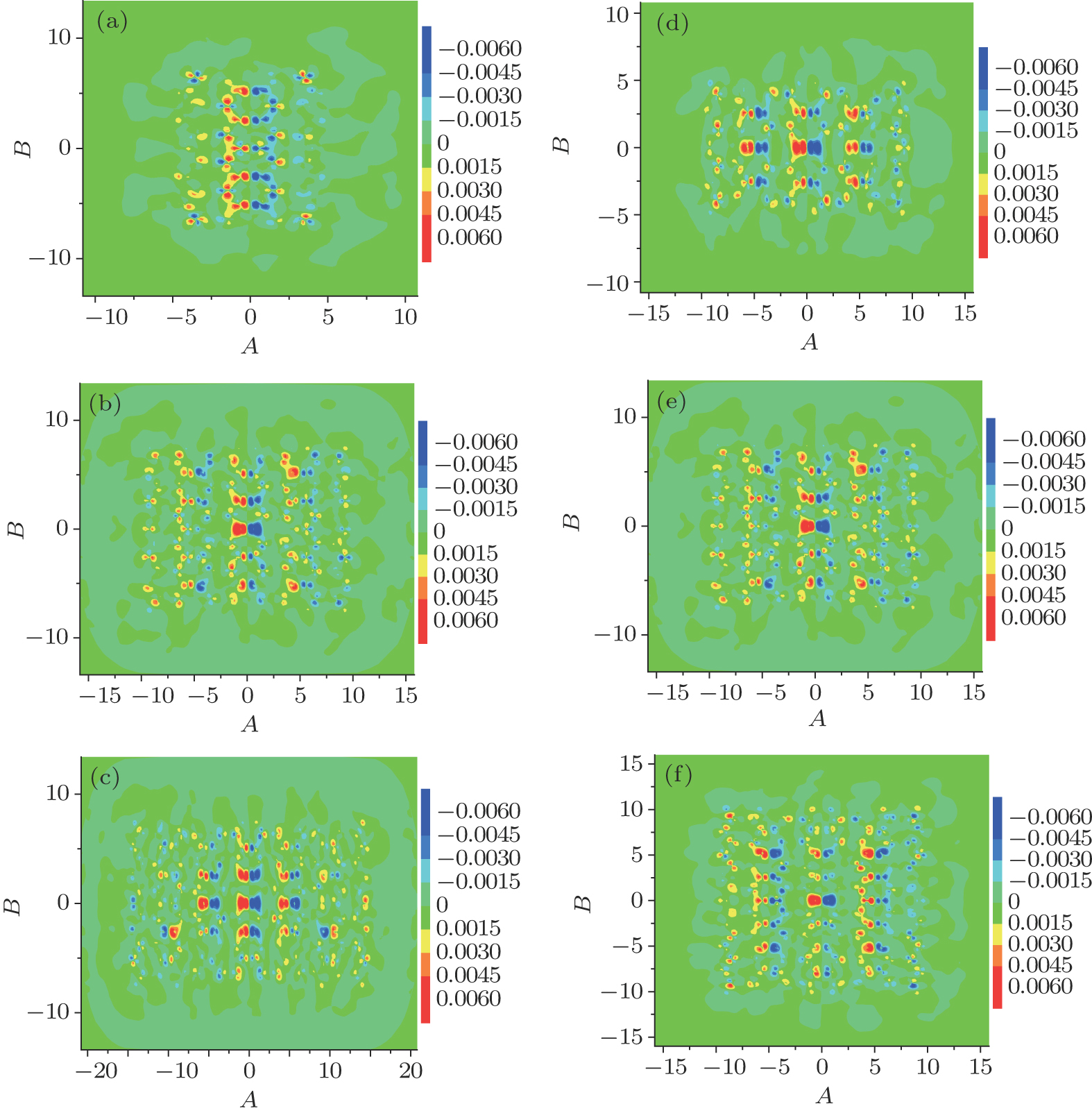
As shown in Fig. 6, we mainly analyze the Fourier transform of induced charge density with 5 types of C2O nanostructures which are mentioned above. The induced charge density plane is parallel to the XY plane, and the incident light polarizes along the armchair-edge at the photon energies of about 7.5 eV, 7.32 eV, 7.3 eV, 7.15 eV, 7.32 eV, and 7.36 eV, respectively. Learning from Fig. 6, we find that there are some common characteristics of the induced charge. Firstly, the induced charges of some electrons and holes are distributed at the boundary.[29] Secondly, we find that the electrons and holes are assembled in the area of two columns of adjacent oxygen atoms, which means that the plasmon resonance modes are of localized excitation.[30] It is different from the long-range charge transfer excitation of graphene. This mode of localized excitation may be caused by the fact that oxygen, which has great bind to ambient electrons, and the electrons and holes are confined in a limited space. Thirdly, we find that the electrons and holes are spatially separated.[31] It is beneficial to the fact that C2O can serve as a photo catalytic material. From Figs. 6(a)6(c), with the width increasing along the armchair-edge direction, the columns of oxygen atoms increases, and the densities of the electrons and holes also increase, which is consistent with the phenomenon that the absorption spectra become stronger. Moreover, the columns of localized excitation are increased. The electrons and holes are assembled in the center, because the center part is affected least by the edge configuration. From Figs. 6(d)6(f), with the increasing width along the zigzag-edge direction, the distributions of induced charge density are basically the same as the distributions of induced charge density in Figs. 6(a)6(c). However, their difference is that the electrons and holes are diffused to the boundary. From the study of the plasmons of C2O nanostructures, it is obvious that we can control the optical response of surface charge by controlling the edge configuration and size.

Fig. 6. (color online) Fourier transformed induced charge densities for rectangular C2O nanostructures 2 × 5, 4 × 5, 6 × 5, 4 × 3, 4 × 5, 4 × 7. For panels (a), (b), (c), (d), (e), and (f), the polarization direction is along the armchair-edge at the photon energies of about 7.5 eV, 7.32 eV, 7.3 eV, 7.15 eV, 7.32 eV, and 7.36 eV, respectively.

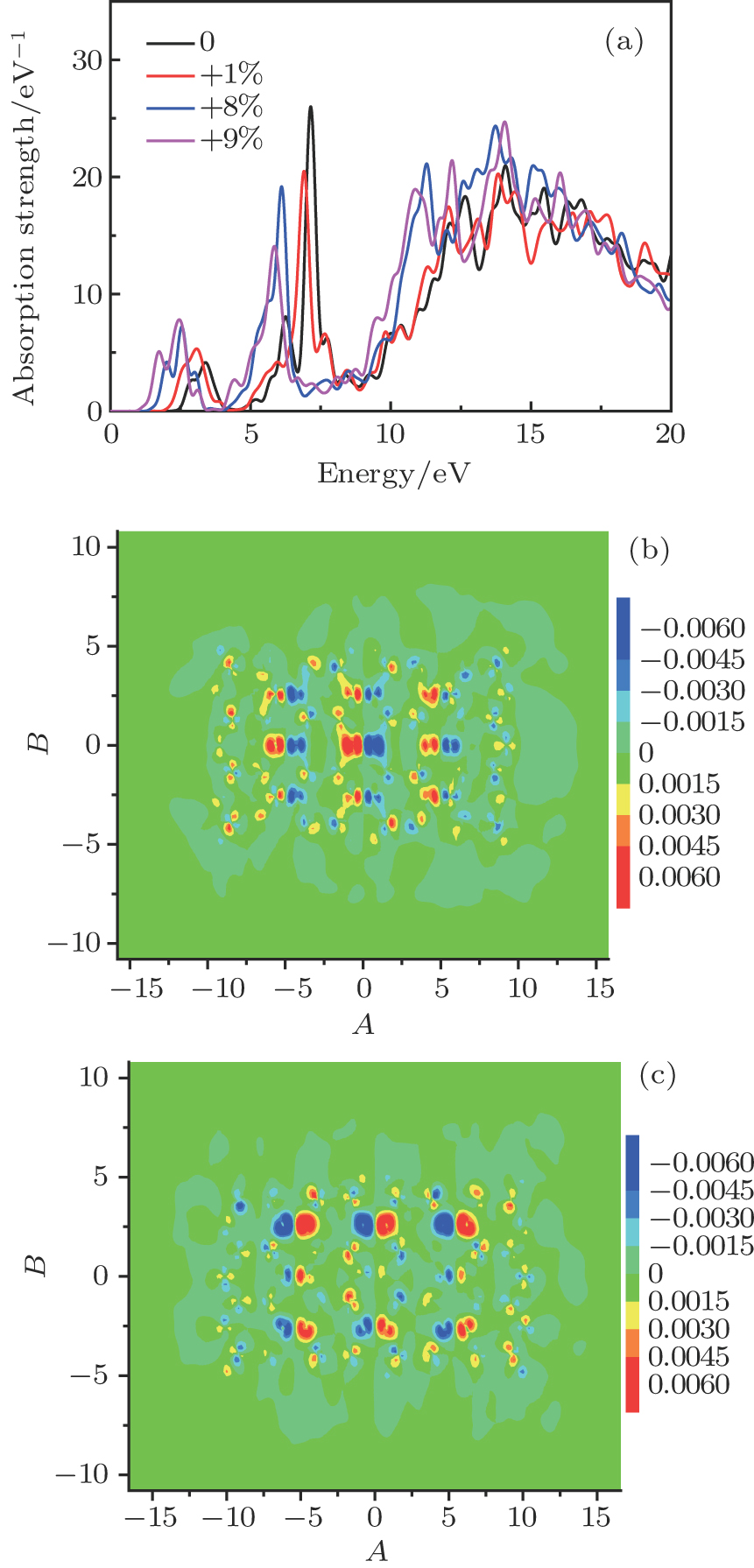
To be applied to a real system, C2O should be grown on a flexible substrate, which may cause a lattice constant mismatch to inevitably occur.[32,33] From many experimental and theoretical studies, we find that the strain has an effect on the optical properties. We can freeze the lattice constants by using the mechanical biaxial strain, which is different from the optimized value. We use η = (aa0)/a0 to represent a biaxial strain, from which a0 represents an optimized lattice constant, and a refers to the lattice length which is along the strain direction.[34] Positive values of η represents the elongation. The band gaps of strained C2O as a function η are presented in Fig. 7(a), and within a strain they are 0, 1%, 8%, 9%, respectively. With the increase of η, we can find that the absorption peak becomes stronger in low-energy region, and the main absorption becomes weaker. In addition, there is a red shift of the resonance point for each of the rectangular C2O nanostructures and an enhanced absorption of visible light. Elongation strain makes the energy gap become wider, and results in the increasing of photonic band gap, therefore, the absorption spectra are red-shifted. The C2O is a material which is sensitive to strain and can be used as a mechanically sensitive material. Moreover, we obtain the Fourier transform of the induced charge density for 4 × 3 rectangular C2O nanostructures. This is a process of gradual change, when the values of η are 0 and 9%. We can easily find the transitional tendency with the optical responses of electrons and holes. For Figs. 7(b) and 7(c) the values of η are 0 and 9%, the incident light polarizes along the armchair-edge at the photon energy points about 7.15 eV and 5.85 eV. From Figs. 7(b) and 7(c), we find that the electrons and holes are assembled in the center, and then diffuse to the boundary. This phenomenon may be caused by the fact that the thickness of C2O becomes thin, and the surface of C2O becomes flat as the value of η increases. Elongation strain has an obvious effect on the C2O nanostructure, which helps us to change the properties of the material.

Fig. 7. (color online) (a) Elongation-strain-induced changes of the absorption spectra of 4 × 3 rectangular C2O nanostructures. Fourier transform of the induced charge density for rectangular C2O nanostructures 4 × 3; ((b) and (c)) Polarization direction is along the armchair-edge at the energy points 7.15 eV and 5.85 eV, respectively, and the values of η are both 0, 9%.
4. Conclusions

In this work, we theoretically predict a highly stable single-layer C2O. We perform first principles simulations to investigate the stability and the electronic structure of C2O. By computing the phonon spectrum, cohesive energy and formation energy, we draw a conclusion that the C2O is kinetically stable. Through analyzing the electronic band structures of C2O and the density of states of C2O, we find this structure is a direct-gap semiconductor. According to TDDFT, we carry out a systematic study of the optical properties of monolayer C2O nanostructure with rectangular geometry. Because of the existence of anisotropy in C2O structure, its absorption spectra show optical anisotropy, which means it would be used as a photoelectric switch. We focus on the optical absorptions of the single-layer C2O nanostructures when the incident light polarizes along the armchair-edge direction. With the increasing of width along the armchair-edge, the absorption strength becomes stronger and the resonance point is red-shifted. In low-energy resonance area, this phenomenon will improve the utilization region of solar energy. With increasing width along the zigzag-edge direction, the absorption strength becomes stronger. The optical properties can be controlled by the edge configuration and size of the C2O nanostructure. In addition, elongation strain also has an effect on the optical properties of C2O nanostructure. With the elongation strain increasing, there is a red shift and the range of absorption spectra become wider. Ours research results reveal that C2O is a promising candidate as a photoelectric material.

Reference
[1] Nie S Emery S R 1997 Science 275 5303
[2] Xu H Bjerneld E J Käll M 1999 Phys. Rev. Lett. 83 4357
[3] Maier S A Kik P G Atwater H A 2002 Appl. Phys. Lett. 81 1714
[4] Yan J Gao S W 2008 Phys. Rev. 78 235413
[5] Hirsch L R Stafford R J Bankson J A 2003 Proc. Nat. Acad. Sci. 100 13549
[6] Bachelier G Russier-Antoine I Benichou E 2008 Phys. Rev. Lett. 101 197401
[7] Brown L V Sobhani H Lassiter J B 2010 ACS Nano 4 819
[8] Yin H F Zhang H 2012 Physica B: Condens. Matter 407 416
[9] Rao C N R Sood A K Subrahmanyam K S 2009 Angewandte Chemie International Edition 48 7752
[10] Allen M J Tung V C Kaner R B 2010 Chem. Rev. 110 132
[11] Yin Y H Niu Y X Ding M 2016 Chin. Phys. Lett. 33 057202
[12] Sun M Ren Q Zhao Y 2017 Carbon 120 265
[13] Sun M L Chou J P Ren Q 2017 Appl. Phys. Lett. 110 392
[14] Kim J Cote L J Kim F 2010 J. Am. Chem. Soc. 132 8180
[15] Suarez A M Radovic L R Bar-Ziv E 2011 Phys. Rev. Lett. 106 146802
[16] Gao W Alemany L B Ci L 2009 Nat. Chem. 1 403
[17] Loh K P Bao Q Eda G 2010 Nat. Chem. 2 1015
[18] Huang B Xiang H Xu Q 2013 Phys. Rev. Lett. 110 085501
[19] Li L Y Yan B P Zhang C M 2012 Acta Phys. Sin. 61 167506 in Chinese
[20] Perdew J P Burke K Ernzerhof M 1996 Phys. Rev. Lett. 77 3865
[21] Segall M D Lindan P J D Probert M J 2002 J. Phys.: Condens. Matter 14 2717
[22] Baroni S de Gironcoli S 2001 Rev. Mod. Phys 73 515
[23] Marques M A L Castro A Bertsch G F 2003 Comput. Phys. Commun. 151 60
[24] Troullier N Martins J L 1991 Phys. Rev. 43 1993
[25] Gerlich D 1993 J. Chem. Soc. Faraday Trans. 89 2199
[26] Liu D Every A G Tománek D 2016 Phys. Rev. 94 165432
[27] Nagare B J 2015 RSC Adv. 5 77478
[28] Yin H Zhang H 2012 J. Appl. Phys. 111 103502
[29] Zhang K Zhang H 2014 J. Phys. Chem. 118 635
[30] Shao L Ruan Q F Li Y 2017 Chin. Phys. 26 036802
[31] Yuan S J Zhang H Cheng X L 2017 Plasmonics 1
[32] Lalmi B Oughaddou H Enriquez H 2010 Appl. Phys. Lett. 97 223109
[33] Vogt P De Padova P Quaresima C 2012 Phys. Rev. Lett. 108 155501
[34] Li J Xu S Zhang J Y 2017 Chin. Phys. 26 036802