|
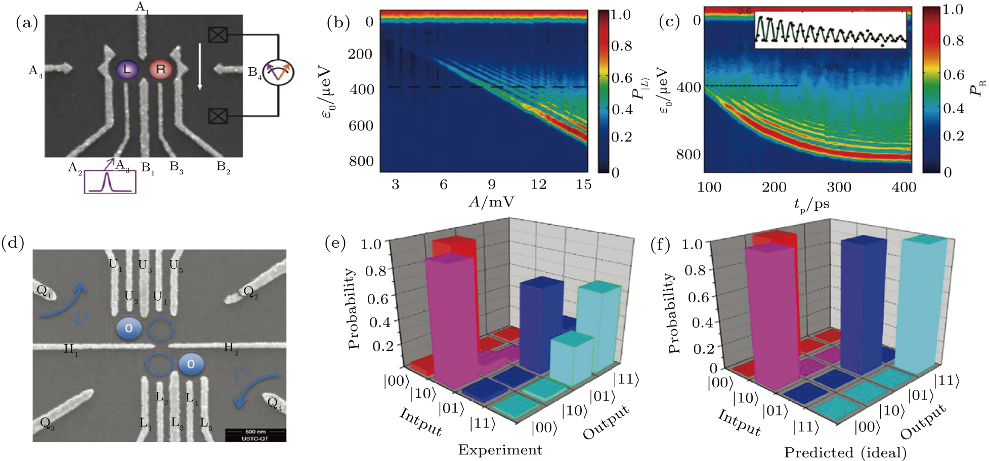
(color online) Experimental demonstration of charge qubit gates.[25,32] Panels (a) and (d) are SEM images for the devices demonstrating one and two qubit gate operations, respectively. Quantum dots are denoted by circles and the
 or
or
 (the conductivity of QPC channel) are shown by arrows. Panels (b) and (c) show the probability of the qubit in the left dot state P|L〉 as a function of the voltage amplitude A and the pulse width
 at different detuning energy position ε0, respectively. These results indicate that both the voltage amplitude and the pulse width can control the rotation to a certain angle at appropriate detuning points, leading to the universal control of charge qubits. The inset of panel (c) shows P|L〉 along the line cut at
 , revealing ultrafast oscillations. Panels (e) and (f) demonstrate the truth table of CNOT operation experimentally and theoretically, respectively. |mn〉 denote the control qubit in the state |n〉 and the target qubit in the state |m〉. The red, pink, blue and green bars correspond to input states |00〉, |10〉, |01〉, and |11〉, respectively.
|