|
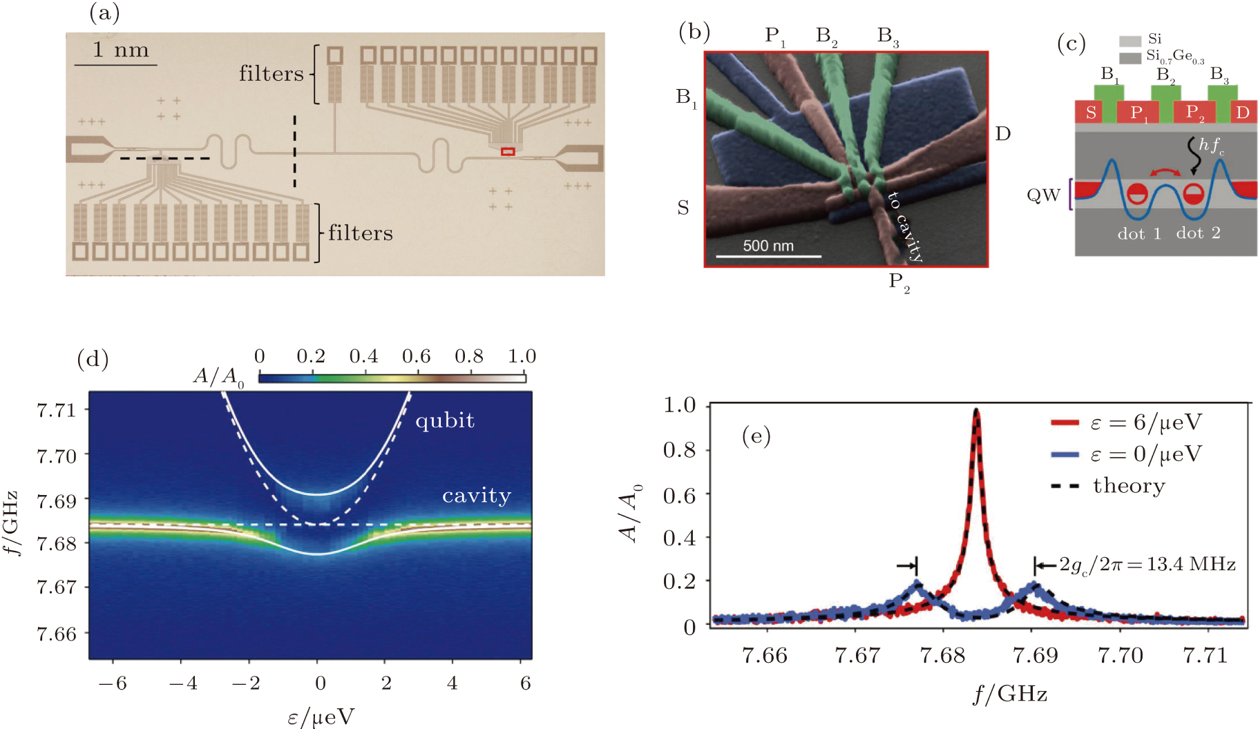
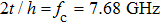
(color online) Experimental demonstration of the hybrid circuit quantum electrodynamics.[83,84] (a) Optical image of a silicon hybrid circuit quantum electrodynamics device that was used to demonstrate strong coupling. An Si double quantum dot indicated by the red box is placed at the voltage anti-node of the cavity. LC filters are used to improve cavity quality. (b) False color SEM image of the Si quantum dot used in panel (a). Gate P2 is used to connect the cavity while playing the role of a plunger gate in the double quantum dot. (c) Schematic cross section of the double quantum dot. An excess electron is confined in the quantum well (QW) denoted by the blue line, while a cavity photon with energy
 interacting with the electron is denoted by a black arrow, where h is the Planck’s constant and
 is the photon frequency. (d) Cavity transmission spectrum
 as a function of photon frequency f and detuning ε with
 , where t is the interdot tunnel coupling. Solid lines are system eigenenergies at the case of
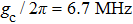 while dashed lines are those of no coupling. (e)
 as a function of f at
 and
and
 . Dashed lines are theoretical predictions. The normal mode splitting shown by two blue peaks indicates the strong coupling regime is reached.
|