Interfaces of high-efficiency kesterite Cu2ZnSnS(e)4 thin film solar cells
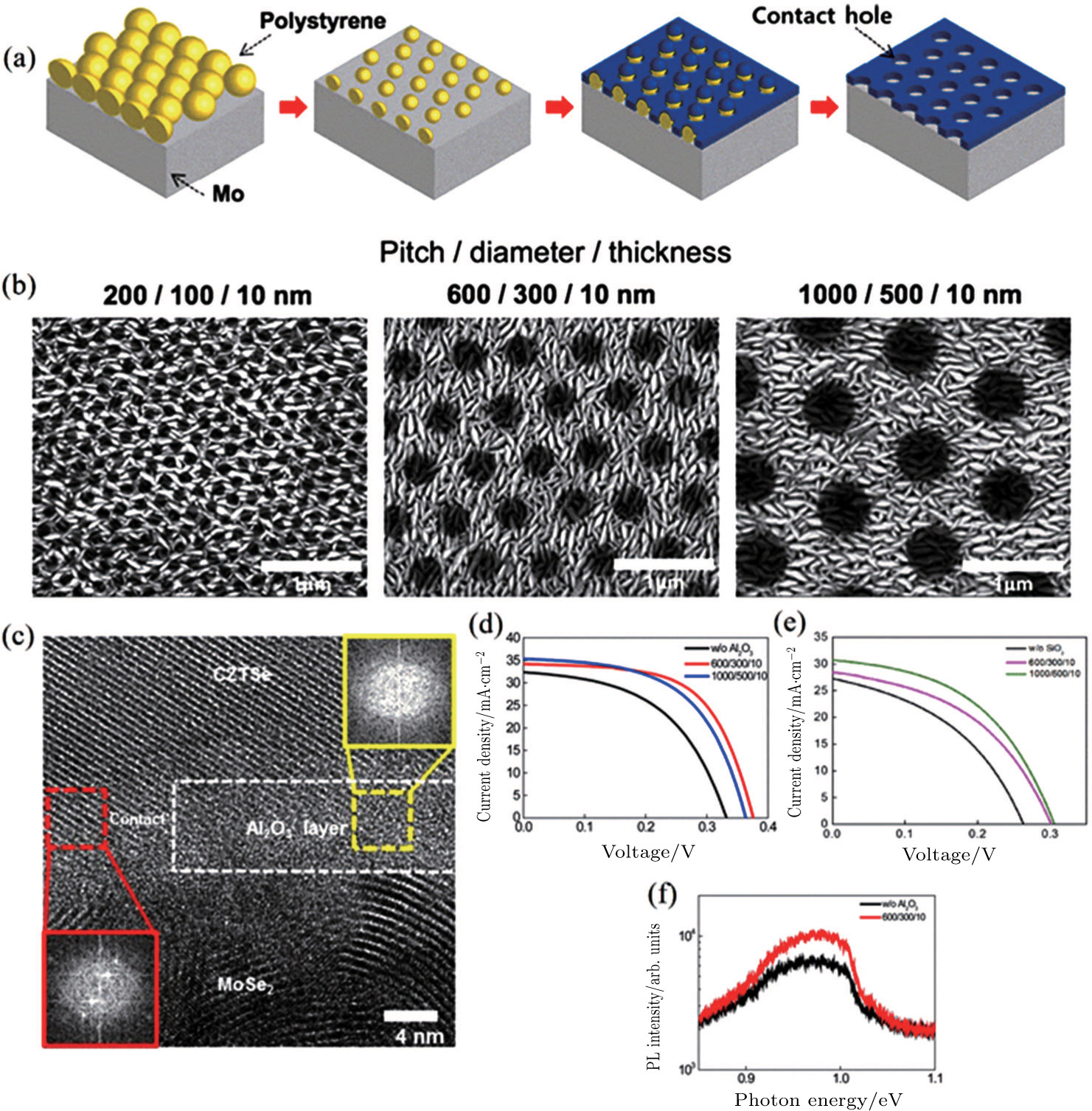
(color online) (a) Schematic drawings of passivation layer with nano-patterned local contacts. (b) SEM images of contact holes on Mo after nanosphere lithography. (c) Cross-sectional TEM image of a bottom Al2O3 passivation layer (white dotted square) with a local contact between CZTSe and MoSe2. Insets are Fourier transform images taken by the area of near the surface (yellow dotted square) and the bulk (red dotted square), respectively. (d) J–V characteristics for the CZTSe solar cells with and wihout a (d) Al2O3 and (e) SiO2 passivation layer at the CZTSe/Mo interface. (f) 10 K photoluminescence spectra of CZTSe solar cells with and without an Al2O3 passivation layer at the CZTSe/Mo interface. Reproduced with permission from Ref. [