Improved performance of Ge n+/p diode by combining laser annealing and epitaxial Si passivation
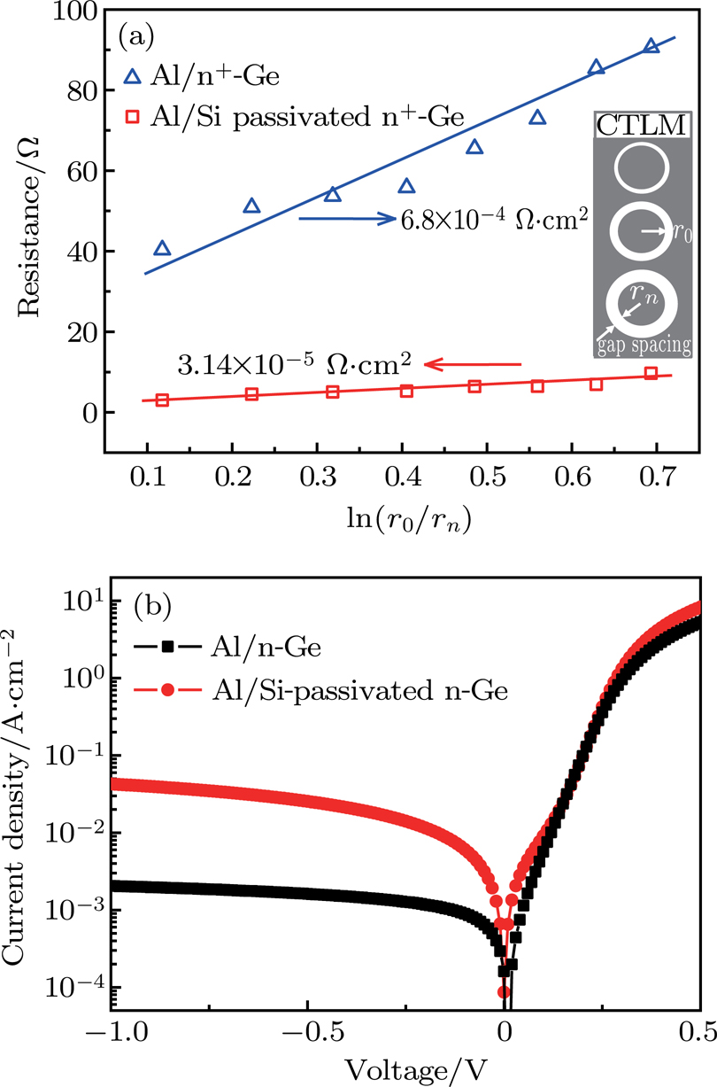
(color online) (a) Dependence of CTLM resistance on gap spacing for Al/n+-Ge contacts. The inset shows the CTLM schematic structure (top view). (b) Current–voltage characteristics of Al/n-Ge contacts with and without Si passivation.
