† Corresponding author. E-mail:
Project supported by the National Natural Science Foundation of China (Grant Nos. 51579057, 5177090655, and 51379052) and the State Key Laboratory of Urban Water Resource and Environment, Harbin Institute of Technology, China (Grant No. 2016DX07).
A new hybrid organic-inorganic structure of FTO/TiO2/Se/HTL/Au based selenium solar cell has been fabricated through a low-cost spin-coating process in air. In this process, selenium is completely dissolved in hydrazine, to form a homogeneous precursor solution. After spin-coating the precursor solution on the TiO2 substrates, following by sintering at 200 °C for 5min, a uniform selenium film with crystalline grains is formed. The selenium based solar cell exhibits an efficiency of 1.23% under AM1.5 illumination (100 mW⋅cm−2), short-circuit current density of 8 mA⋅cm−2, open-circuit voltage of 0.55 V, and fill factor of 0.37. Moreover, the device shows a stable ability with almost the same performance after 60 days.
Selenium (Se) based inorganic-organic heterojunction solar cells have been considered as one of the most promising candidates for solar energy harvesting.[1–3] Se can be used as a photoabsorber to generate photoelectrons in solar cells due to its stable nature and suitable band gap of 1.8 eV.[4] The maximum theoretical efficiency of selenium-based solar cells estimated to be about 20% under AM1 from the band gap energy of crystalline selenium.[5] Many studies on this type of selenium solar cell have been reported. ITO et al. assembled Se-based solar cells with a high efficiency of 5.01% and promising features early in mid-1980s.[6] Recently, a type of solar cell in ITO/compact-TiO2/mp-TiO2/Se/Au structure based on an extremely thin Se absorption layer on mesoporous TiO2(mp-TiO2) is successfully constructed with an over 3% power conversion efficiency (PCE) without any expensive organic parts.[7]
Although very impressive cell efficiencies have been achieved, the cell architecture, use of vacuum, or the two-step deposition process should be modified to improve efficiency and reduce fabrication costs since the high vacuum condition is high energy consumption and low production capacity. Evaporation process during fast spinning can induce the formation of well-crystallization between Selenium and the substrate for the fast crystallization rate of Se, which often leads to a poor coverage and morphology.[8,9]
Spin coating, as one of the cheapest film production methods, is widely used in solution-processed solar cells.[10] Alternatively, solution-based techniques have been proposed to fabricate thin films using a mixture of two precursors to form the complete absorption layer. Therefore, a high-quality Se films using mixing solvent is successfully prepared through spin-coating process in the ambient condition.[11] It is significative to synthesize Se film in the ambient condition without glove box involved.
Herein, we report a successful application of a solvent method for selenium film in heterojunction solar cell under air atmosphere. This solvent-engineering technology enabled fully solution-processed selenium based inorganic-organic heterojunction solar cells with a certified 1.23% PCE under standard reporting conditions. Comparing with the different hole transport materials (HTM) for this structure device, it provides important progress towards the understanding of the role of solution processing under air atmosphere in the realization of low cost and highly efficient selenium based inorganic-organic heterojunction solar cells.
The titanium (IV) isopropoxide (TTIP) was purchased from Aladdin. Other anhydrous solvent was purchased from Alfa Aesar. 4-tert-butypyridine and lithium bis(trifluoromethanesulfonyl)imide (Li-TFSI) were purchased from Kanto. Poly [bis(4-phenyl) (2,4,6-trimethylphenyl)amine] (PTAA) and Poly(3-hexylthiophene-2,5-diyl) (P3HT) were obtained from Sigma-Aldrich. 2,20,7,70-tetrakis-(N,N-di-4-methoxyphenylamino)-9,90spirobifluorene(spiro-OMeTAD) were obtained from Youxuan Trade and Toronto Technologies Co., Ltd, respectively. All chemicals and reagents were used as received without any further purification.
Fluorine-doped tin oxide (FTO) glasses were etched by zinc powder and 2 M hydrochloric solution, following by ultrasonically cleaning in deionized water, detergent solution, ethyl alcohol and acetone for 30 min, respectively. Then the glasses were transferred to the ultraviolet-ozone (UV-O3) cleaner and kept for 15 min. Subsequently, a titanium isopropylate (TTIP) solution including TTIP (369 μL) and 2.53 mL 2-propanol (IPO) was spin-coated on surface of the cleaned fluorine-doped tin oxide glasses (FTO), and calcined at 450 °C for 1 h, and the compact layer of TiO2 (about 80 nm in thickness) was obtained. Lastly, a 200–300 nm thick mesoporous TiO2 (mp-TiO2) film was formed on the compact TiO2/FTO substrate after spin-coating the pastes and calcining at 500 °C for 30 min.
300 mg⋅mL−1 selenium hydrazine solution was spin-coated onto the as-prepared mp-TiO2/compact TiO2/FTO substrates with the different hot casting temperature from 25 to 175 °C at speed of 2000 r.p.m. for 30 s. After sintering at 200 °C for 5 min, a black crystalline Se layer was obtained. Subsequently, the P3HT, spiro-OMeTAD and PTAA as hole transport materials (HTMs) were spin-coated on the Se layers respectively. Finally, a gold counter electrode was prepared by thermal evaporation deposition. The active area was fixed at 0.12 cm2.
The morphology of Se films were characterized by field-emission scanning electron microscopy (FEI HELIOS NanoLab 600i). The crystal structure and phase purity of the Se films were investigated by x-ray diffraction (XRD) using a Empyrean Panalytical X’Pert Pro x-ray diffractometer with Cu Kα radiation 1.5418 Å. The band gap of Se films was studied through UV-visible (UV-vis) absorption spectra using a spectrophotometer equipped with an integrating sphere setup (UV-3600). The current density–voltage (J–V) characteristics of these devices were obtained on a comprehensive electrochemical power workstation (VersaSTAT3, Ametek, USA).The photovoltaic performance was recorded under AM1.5G illumination at a calibrated intensity of 100 mW⋅cm−2 with the Newport 94021A class ABB solar simulator equipped with a 150 W xenon lamp. The illumination intensity was standardized before each test by a standard Si solar cell (1218, Newport, USA).
Schematic of the simple solution spin coating proceed methods of Se film and Se based solar cells deposition is shown in Fig.
 | Fig. 1. (color online) Schematic illustration of different steps in solution processed methods for Se-based solar cells. |
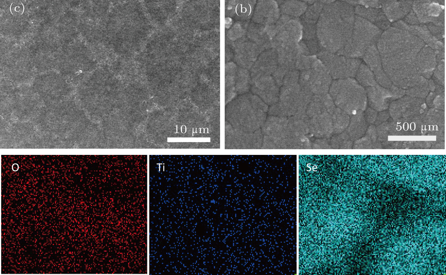
Figure
 | Fig. 2. (color online) Top-view SEM images of the Se crystalline film coated on FTO/TiO2 substrate at (a) low and (b) high magnifications and EDX analysis of FTO/TiO2/Se films with elemental mapping. |
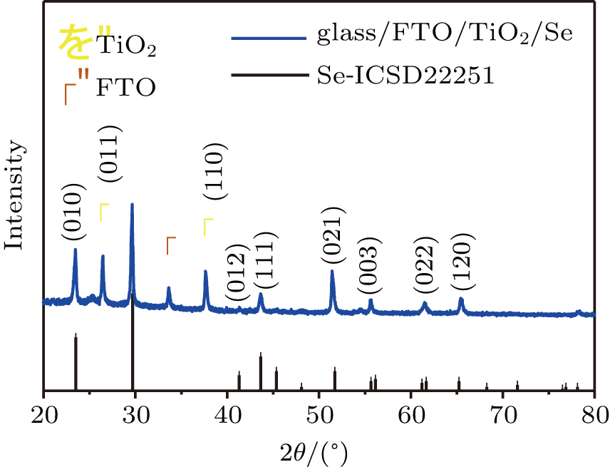
Photoabsorption and the transmission of electrons are significantly affected by the crystallinity and morphology of the inorganic photoabsorber. In this work, Se films annealed at 200 °C for 5 min, the crystal structure of the Se film annealed at 200 °C for 5 min is characterized by XRD (Fig.
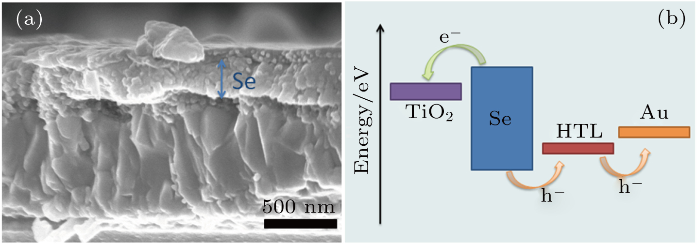
In this study, we used Se as a photoabsorber to design organic-inorganic Se-based solar cells with a FTO/compact-TiO2/mp-TiO2/Se/HTL/Au structure (Fig.
 | Fig. 4. (color online) Cross-sectional SEM image of a complete device (a) and energy level diagram of Se-based solar cells (b). |
The ultraviolet visible (UV-vis) absorption spectra of selenium films deposited on TiO2/FTO are shown in Fig.
 | Fig. 5. (color online) UV-vis absorption spectra of Se film (a) and J–V curves of Se-based solar cells (b). |
Figure
| Table 1.
Photovoltaic parameters of the optimized Se-based solar cell with different HTL under AM 1.5 G irradiation (100 mW⋅cm−2) of the corresponding device. . |
Figure
In summary, inorganic-organic heterojunction solar cells have been fabricated employing a Se film as the photoabsorber layer, which is prepared by facile spin-coating method in ambient condition. A new selenium thin-film solar cell has been developed. The unoptimized selenium based thin-film solar cell in FTO/TiO2/Se/HTL/Au structure exhibits PCE of 1.23%, AM1 of 100 mW⋅cm−2 and an efficiency of 1.07% after aging for 60 days. This new type of Se-based solar cell from a facile spin coating method under ambient condition with satisfied performance make it possible to fabricate competitive solar cell in low cost process.
| [1] | |
| [2] | |
| [3] | |
| [4] | |
| [5] | |
| [6] | |
| [7] | |
| [8] | |
| [9] | |
| [10] | |
| [11] |


