


Importance of PbI2 morphology in two-step deposition of CH3NH3PbI3 for high-performance perovskite solar cells
Cite this Article
Wei Hui, Tang Yang, Feng Bo, You Hui. Importance of PbI2 morphology in two-step deposition of CH3NH3PbI3 for high-performance perovskite solar cells. Chinese Physics B, 2017, 26(12): 128801 
Permissions
Importance of PbI2 morphology in two-step deposition of CH3NH3PbI3 for high-performance perovskite solar cells
† Corresponding author. E-mail:
Abstract
Controlling the morphology of the perovskite film is an effective way to improve the photoelectric conversion efficiency of solar cell devices. In this work, we study the influence of the crystallization condition on PbI2 morphology and the performances of resulting perovskite solar cells. The PbI2 morphologies and coverage rates under different formation conditions such as solvent effect, slow crystallization at room temperature and substrate-preheating, are found to be of crucial importance for preparing high-quality perovskite. The generation of loosely packed disk-like PbI2 film with interpenetrating nanopores promotes the penetration of methyl ammonium iodide (MAI), leading to a better crystallinity of the perovskite film, and a best repeatable power conversion efficiency of 11.59% is achieved when methyl ammonium lead triiodide (CH3NH3PbI3, MAPbI3) is employed. In addition, an excellent device is also obtained with an efficiency of more than 93% to remain after working for 43 days.
1. Introduction
Hybrid organic–inorganic perovskite, the chemical general formula ABX3 (A = CH3NH3, HC(NH2)2, Cs; B = Pb, Sn; X = Cl, Br, I) perovskite family, is a well-known material with excellent absorption coefficient,[1,2] long carrier diffusion length,[3–5] high mobility,[6,7] and a tunable bandgap.[8–10] These properties can be tuned by changing the A, B, and X atoms. Nowadays, the certified efficiency of a hybrid organic–inorganic perovskite solar cell (PSC) has already reached up to 22.1%,[11] which proves that the hybrid organic–inorganic perovskite is a viable candidate for crystalline silicon solar cells and copper indium gallium selenide (CIGS) commercial photovoltaic (PV) devices, owing to its low-cost and facile solution-based fabrication process.
The perovskite film is at the core of PSC, whose quality greatly determines the photovoltaic performance. Many photo-physical properties, such as light harvesting, charge carrier transport and diffusion length, can be dramatically affected by the crystallization of the perovskite.[12–14] The defects and the crystal grain boundaries of the perovskite crystallites act as the traps of carriers, which aggravate the charge recombination. The current density–voltage (J–V) hysteresis effect, which causes inaccuracy in evaluating cell efficiency, is also believed to be related to the crystallinity and interfaces of the perovskite.[15,16] Thus, the performance of perovskite solar cell strongly depends on the morphology and composition.[17–22] So far, many methods have been exploited to prepare perovskite films with excellent photon and electron properties through tuning nucleation growth and the resulting micro-morphology of perovskite films.[23] Compared with the one-step method, the two-step method offers the good controlling of morphology, and it is much more economical and convenient than the vapor deposition method. For the two-step method, an inorganic halide (e.g., lead (II) iodide, PbI2) layer is first deposited, whereupon organic ions (e.g., methyl ammonium iodide, MAI) are intercalated between the layers of edge sharing PbI6 octahedra and form the perovskite. Burschka et al. used this two-step method to fabricate a perovskite solar cell in 2013,[24] wherein the spin-coated and dried PbI2 layer was dipped in an appropriate 2-propanol solution with MAI. The process for PbI2 deposition in the sequential deposition was found to be crucial to the final MAPbI3 morphology and photovoltaic performance.[25] As a perovskite inorganic framework, the morphology of the original PbI2 may affect the reproducibility of the photovoltaic performance because high-quality perovskite thin film depends on the morphology of the PbI2 layer, dipping time, concentration and temperature of the MAI solution. In addition, the MAI penetration is a serious issue due to the volume expansion when the MAI is inserted into the PbI2 crystal lattice.[25,26] This will lead to incomplete transformation of PbI2 to perovskite on account of the fact that the initially formed MAPbI3 compact layer blocks the MAI from being diffused and inserted into the PbI2 layer. Moreover, the residual PbI2 has detrimental effects on the carrier separation and transportation. In the present work, we fabricate the materials with different surface morphologies (mainly surface coverage and different roughness) by adjusting the drying process of the PbI2 layer.[26] Then the influences of synthesis conditions on the microstructures of perovskite films and the optical-electrical performances of the cells are investigated.
2. Solar cell fabrication
Patterned fluorine-doped tin oxide (FTO) substrates were cleaned in the solvents of detergent solution, acetone, ethanol and deionized water sequentially. Then the cleaned substrates were treated by UV-O3 for 15 min to make them well hydrophilic. After that, 50-nm thick compact TiO2 (c-TiO2) was formed on the cleaned FTO glass by spin-coating 0.15-M solution of titanium diisopropoxide bis (acetylacetonate) (75 wt% in isopropanol, Aldrich) in 1-butanol (99.8%, Aldrich) at 3000 r.p.m for 30 s, which was dried at 125 °C for 5 min, then the process was repeated once again. A mesoporous TiO2 (m-TiO2) layer composed of 20 nm-sized particles was deposited by spin-coating at 3000 r.p.m for 30 s by using a commercial TiO2 paste (18-NRT, Dyesol) diluted in ethanol (2:7, weight ratio). After drying at 125 °C for 10 min, the substrate was annealed at 500 °C for 30 min.
2.1. PbI2 layer fabrication
PbI2 (99.99%, Sigma-Aldrich) was dissolved in several kinds of polar solvents (N, N-dimethylformamide, DMF, 
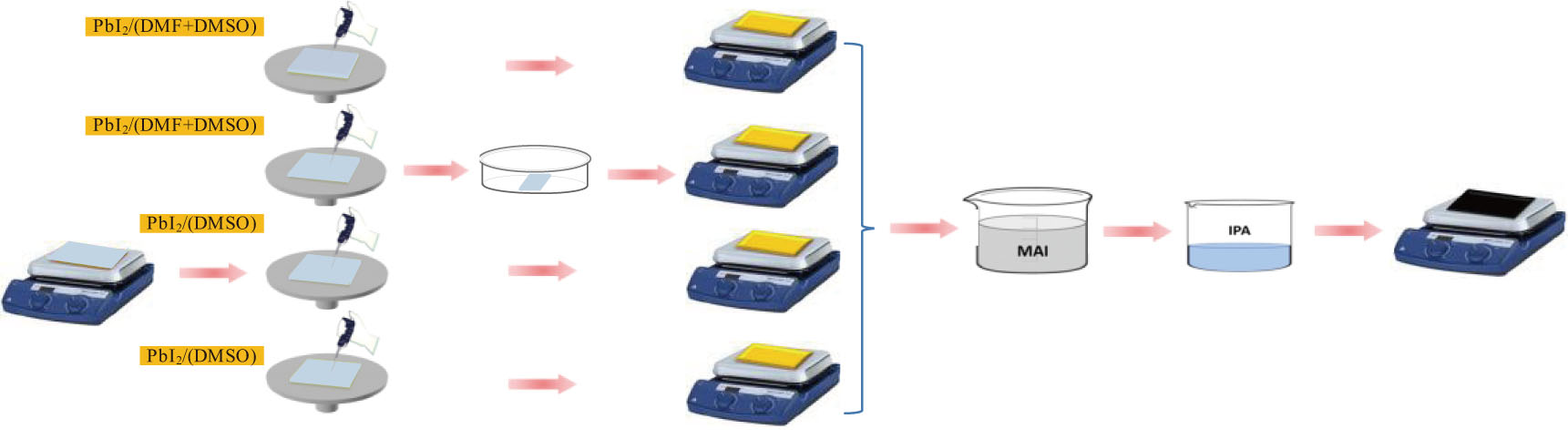 | Fig. 1. (color online) A schematic diagram representation of the fabrication process. |
| Table 1.
The PbI2 precursor films prepared with different processes. . |
2.2. MAPbI3 layer fabrication
To convert the PbI2 layer into MAPbI3, after cooling the substrates to room temperature, PbI2 films were dipped into a solution of CH3NH3I (MAI, 


2.3. Characterization
The x-ray diffraction measurements were performed on the D8 DISCOVER diffractometer (Bruker D8D, Germany) in grazing incidence x-ray diffraction (GIXRD) mode. The XRD patterns in a range from 10° to 60° were recorded at room temperature by using Cu Kα radiation under the following measurement conditions: a tube voltage of 40 kV, tube current of 40 mA, step size of 0.04°, and 20 s per step. The value of the grazing incidence angle was 0.05°. The absorption spectra of perovskite films were characterized by a UV-Vis-NIR spectrophotometer (SHIMADZU, UV3600) with an integrating sphere in the interval of 600 nm–900 nm. The photoluminescence (PL) spectra were measured by using an integrated Raman system (Horiba Jobin Yvon LabRam HR-800) with an Olympus 10X lens (
3. Results and discussion
The PbI2 morphology-related reaction kinetics in the two-step method is assigned to heterogeneous nucleation, which leads to the formation of PbI2 nuclei on the m-TiO2 stack layers. The liquid nature of the film, augmented by the presence of a large amount of solvent, leads to subsequent crystal growth, where the extent of growth is controlled by adjusting the nucleation density and growth condition. Figure
 | Fig. 2. SEM images of PbI2 fabricated with method A, B, C, and D, respectively. |
The DMSO acts as both a solvent and a coordination reagent in the formation of a complex of PbI2·DMSO, while DMF behaves only as a solvent with a higher evaporation rate than DMSO (vapor pressure data are listed in Table
| Table 2.
Typical physical parameters for DMF and DMSO solvents used for PbI2 precursor. . |
A series of MAPbI3 films is prepared from different PbI2 precursor films. For comparison, these perovskite thin films are denoted as PSC-a, PSC-b, PSC-c, PSC-d, respectively. Figure 
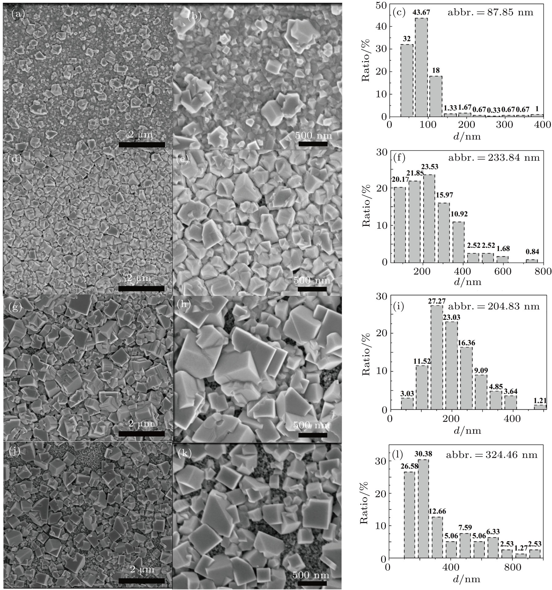 | Fig. 3. SEM images of MAPbI3 fabricated with different methods. ((a) and (b)) MAPbI3 fabricated with method A; (c) the size analysis of the sample shown in panel (b); ((d) and (e)) MAPbI3 fabricated with method B; (f) size analysis of the sample shown in panel (e); ((g) and (h)) MAPbI3 fabricated with method C; (i) size analysis of the sample shown in panel (h); ((j) and (k)) MAPbI3 fabricated with method D; (l) size analysis of the sample shown in panel k. |
In brief, the drying process at room temperature enhances the formation of larger pores in the PbI2 film and larger MAPbI3 particles, indicating the complete transformation of PbI2 into MAPbI3. In the case of pure DMSO used (PSC-c and PSC-d), the MAPbI3 films are mainly composed of large crystals (

Taking it into consideration that the reaction between PbI2 and MAI is a solid–liquid reaction, we believe that the reaction rate is determined by three major factors: (i) property of PbI2 film, such as preferential orientations of crystal, crystallinity and morphology of PbI2 precursor film; (ii) concentration of MAI/IPA solution; (iii) temperature of the reaction system. In our study, the latter two factors have been carefully controlled. So we believe that the great difference among PbI2 films in the preparation of perovskite comes from the morphology difference as shown in Fig.
In general, GIXRD is an effective tool to determine the surface crystallinity by changing the incident angle of x-ray. The samples are kept in a carefully controlled measurement condition, so the diffraction peak intensity is mainly determined by the crystallization, densification and components of the sample. The GIXRD patterns of the MAPbI3 films obtained from PbI2 are shown in Fig.
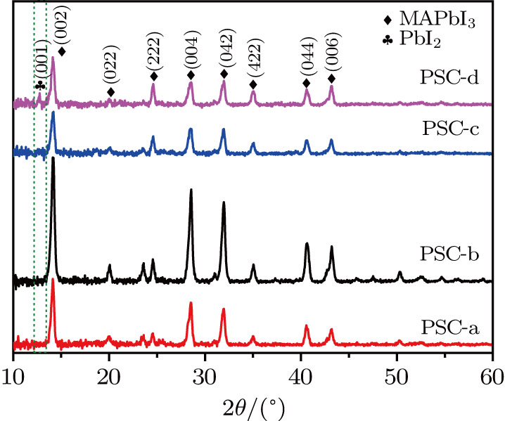 | Fig. 4. (color online) XRD patterns of MAPbI3 fabricated with methods A, B, C, and D, respectively. |
The higher intensity in the PSC-b film should be attributed to the slight thickness of the sample, or uniformly distributed nanocrystals and complete crystallization of the sample. Furthermore, the slight differences in lattice constant and full widths at half maximum (FWHMs) for different films imply that the PbI2 precursor film only influences the perovskite film coverage and morphology without causing significant changes in the crystalline structure of the material.
Table 

| Table 3.
Lattice constants of MAPbI3 films. . |
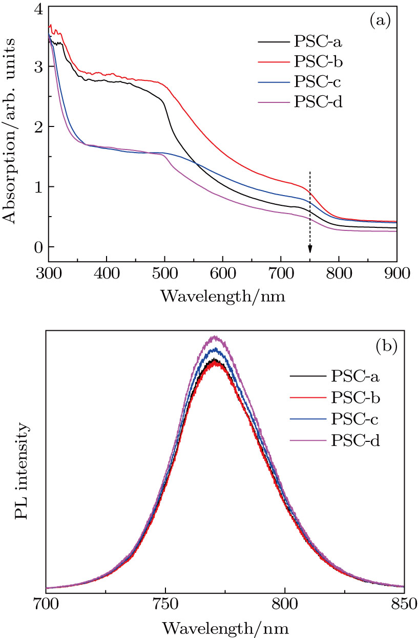
Figure
 | Fig. 5. (color online) (a) Absorption spectra and (b) PL spectra of MAPbI3 films. |
The photovoltaic performances of the fabricated PSCs based on FTO/c-TiO2/m-TiO2/MAPbI3/HTM/Ag architecture are examined and the current–voltage (J–V) characteristics are measured in the reverse bias condition (


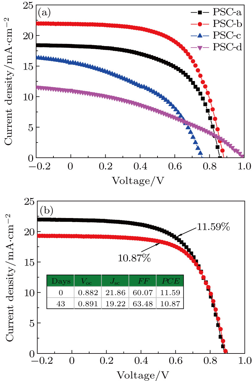 | Fig. 6. (color online) (a) J–V curves of devices fabricated with different methods. (b) J–V curves of the best performance device fabricated by method B. |
| Table 4.
Photovoltaic parameters of devices with different fabrication methods. . |
For mixed solvents, the higher PCE of PSC of the material prepared by method B is attributed to the PbI2 scaffold with mesoporous structure, which promotes the conversion process of and less damage to perovskite. In addition, many studies have shown that a larger perovskite grain size can reduce the interfacial area, which can hinder charges from being collected. Larger grains also possess less bulk defects and higher mobilities, so the photo-generated carriers could be collected more easily.[27,28] We note that Yi et al.[29] reported solar cells based on bilayer porous lead halide (PbX2, containing PbI2 and PbBr2) films prepared by using PbX2 solutions of DMF/DMSO mixed-solvent. The MAI solution can easily diffuse through the PbI2 film and react with PbI2 more completely because of the continuous mesoporous structure. At the same time, these pores also provide the space needed to accommodate the large volume expansion and the insertion of the organic cations into the PbI2 lattice. The interpenetrating nanoporous morphology enables fast penetration of the MAI solution during the conversion step, and perovskite grains can grow freely and form a compact MAPbI3 film. For pure DMSO solvent, PCE of 3.92% is achieved without pre-heating and increases to 5.22% when the substrate is heated to 80 °C. The pre-heating treatment can lead to the increase of photocurrent and voltage. By contrast, the PbI2-DMSO based device suffers relatively low 
4. Conclusions
In this work, a suitable polarity solvent, processed with and without drying at room temperature, pre-heating process of substrate for PbI2 deposition in the two-step coating procedure, and the affinity to PbI2, can facilitate the formation of mesoporous PbI2 films and the fabrication of a uniform and crystalline perovskite film. In the case of full coverage and less pinholes of the perovskite film, excellent device efficiency and stability are achieved successfully. Meanwhile, the PCE of PCS-b keeps a high level of more than 93% (from 11.59% to 10.87%) after the cell has been used for 43 days under ambient conditions.
Acknowledgment
The authors thank the postdoctoral research station of the Hefei Institute of Physical Science for their technical support.
Reference
| [1] | |
| [2] | |
| [3] | |
| [4] | |
| [5] | |
| [6] | |
| [7] | |
| [8] | |
| [9] | |
| [10] | |
| [11] | |
| [12] | |
| [13] | |
| [14] | |
| [15] | |
| [16] | |
| [17] | |
| [18] | |
| [19] | |
| [20] | |
| [21] | |
| [22] | |
| [23] | |
| [24] | |
| [25] | |
| [26] | |
| [27] | |
| [28] | |
| [29] |