Tuning electronic properties of the S2/graphene heterojunction by strains from density functional theory
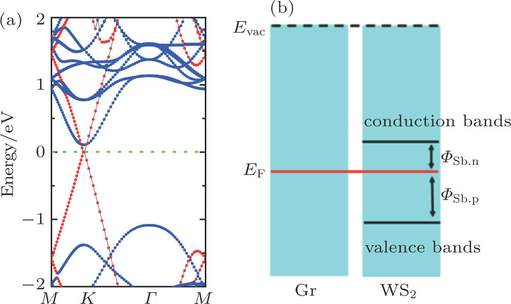
(color online) (a) Electronic band structures of WS2/graphene heterostructure at the equilibrium distance. The blue and red line denote the contributions from WS2 monolayers and graphene, respectively. The Fermi level is set to be zero and marked by green dotted lines. (b) Schematic diagram of the Gr/WS2 interface contact. The n-type (p-type) Schottky barrier height is the energy difference between the CBM (VBM) and the Fermi level.
