† Corresponding author. E-mail:
Project supported by the Fund from Xi’an High-tech Institute, China.
Superlattices in chaotic state can be used as a key part of a true random number generator. The chaotic characteristics of the signal generated in the superlattice are mostly affected by the parameters of the superlattice and the applied voltage, while the latter is easier to adjust. In this paper, the model of the superlattice is first established. Then, based on this model, the chaotic characteristics of the generated signal are studied under different voltages. The results demonstrate that the onset of chaos in the superlattice is typically accompanied by the mergence of multistability, and there are voltage intervals in each of which the generated signal is chaotic.
Random number generator (RNG) has been widely used in the fields of scientific research, information processing,[1] national defense and security,[2] etc. Physical systems exhibiting fast spontaneous chaotic oscillations are used to generate high-quality true random sequences in random number generators.[3] Recently, high frequency chaotic oscillations of a semiconductor superlattice under room temperature were found, and it is considered to be an excellent noise source, which makes the superlattice an ideal candidate for true random number generation. A semiconductor superlattice consists of a periodic sequence of thin layers of different types of semiconductor materials. It was first proposed by I Kanter et al. and W Li et al.[4,5]
Specifically, a superlattice is a cyclic structure of coupled quantum wells, where at least two types of semiconductor materials with different band gaps are stacked on their top along the said direction in an alternating fashion.[6,7] For a structure composed of two materials, e.g., GaAs and AlAs, the regions of GaAs serve as quantum wells while those of AlAs are effectively potential barriers. As a result, the conduction band of the whole system exhibits spatially periodic modulation with the period given by the combination of width of the quantum well and the barrier, which is typically much larger than the atomic lattice constant. If the widths of the barriers are sufficiently small, then the quantum tunneling effectively forms a one-dimensional energy band in the growth direction.[8–11]
The quality of the true random number is determined by the chaotic signals generated by the superlattice. Thus, the first step is to study the influence of the signal generation system on the output chaotic signal. There are numerous parameters that can affect the chaotic characteristics of the output chaotic signals, and in principle, all of the system parameters can be adjusted. Experimentally, certain parameters are not readily susceptible to changes, especially those characterizing the materials properties. What could be adjusted are the parameters associated with the driving direct current (DC).
In this paper, we first establish the model of the superlattice. Then, based on this model, the chaotic characteristics of the generated signal are studied under different voltages. The results demonstrate that the onset of chaos in the superlattice is typically accompanied by the emergence of multistability, and there exist voltage intervals in each of which the generated signal is definitely chaotic.
In weakly coupled superlattices in which sequential resonant tunneling is the main transport mechanism, chaos can arise and its potential use as a random number generator has been proposed.[12–14] In this paper, the focus is placed on the strongly coupled regime, in which miniband conduction is the primary contribution to transport.
Using the force-balance equation[15] for an n-doped semiconductor quantum-dot superlattice, we write the dynamical equation for the electron center-of-mass velocity Vc(t) as
Within the tight-binding model, the single-electron kinetic energy εk in a semiconductor quantum-dot superlattice can be written as


For numerical calculations, it is convenient to use dimensionless quantities. Specifically, we introduce 


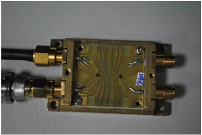
In the experiment, the superlattice used in this study is designed by the Suzhou Institute of Nano-Tech and Nano-Bionics (SINANO), Chinese Academy of Sciences. The encapsulation of the superlattice is shown in Fig.
The measurement system is built as shown in Fig.
When the applied DC voltage equals 2.5 V, the output chaotic signal is measured as shown in Fig.
The basic characteristics of the chaotic dynamics are extremely sensitive to the initial condition. Trajectories of two close initial conditions will separate (or get close) exponentially. Lyapunov exponent is the quantitative description of the phenomenon. For an n-dimensional dynamic system, there usually exist n Lyapunov exponents, which are referred to as the Lyapunov spectrum of the system. The smallest Lyapunov exponent determines how fast the trajectory contracts, while the largest Lyapunov exponent determines the divergence rate. In reality, it is not necessary to calculate all the Lyapunov exponents of the system as the calculation of the largest Lyapunov exponent is enough. As long as the largest Lyapunov exponent is larger than zero, the existence of chaos can be determined. The largest Lyapunov exponent of the superlattce system can be calculated from the phase space reconstructed from the output time series. In this paper, the method proposed by Wolf is used to calculate the largest Lyapunov exponent of the superlattice,[18] and the result is LEmax = 3.256, which shows that the chaotic state definitely exists.
The applied voltage is then adjusted, the results show that there are several voltage intervals in which the outputs of the superlattice are chaotic, while in the other intervals the outputs are determined. It means that the applied voltage of the superlattice is one of the most important parts in the design of the chaotic random number generators using superlattice. While in the past, these voltage intervals are always determined by experiences, in this paper we use the model in Eq. (
Equation (
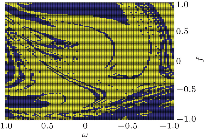
The study of the influences of the superlattice parameters on the output chaotic signal is also important, e.g. it would benefit the design process of the superlattice, and give a directive suggestion for the design of the chaotic superlattice. Thus, the influence of parameter a1 is studied as an example. First, a1 is set to be a1 = 1.8, and other parameters are set to be a0 = 2.1, a2 = 0, b1 = 0.18, b2 = b3 = 0.0018, and ΩC = 1.2. The largest Lyapunov exponents of the system in the plane (v0 = − 1, − 1 ≤ ω0 ≤ 1, − 1 ≤ f0 ≤ 1) are calculated as shown in Fig.
Figure
 | Fig. 5. (color online) Points in the f–ω plane whose largest Lyapunov exponents are larger than zero when a1 = 1.8. |
As a1 changes, the areas that would eventually enter into a chaotic state will also change. Figure
 | Fig. 6. (color online) Points in the f–ω plane whose largest Lyapunov exponents are larger than zero when a1 = 2.4. |
As mentioned above, parameters associated with the DC field are easier to adjust. Figure
In the reality, when the chaotic characteristic of the superlattice is used to generate true random numbers, there are several stages of the parameter design, which should be taken into consideration. In the stage of the fabrication of the superlattice, the influences of the superlattice parameters on the output chaotic characteristics should be first studied. The parameters should be set, for the output signal is easier to be chaotic and has the expected characteristics. Then, in the use of the superlattice, outer conditions like the voltage and current of the superlattice should be considered first to assure that the output has the ideal characteristic. So, the study of how the parameters of the superlattice itself and the external factors affect the chaotic characteristics of the output signal is important and will guide the fabrication and use of the superlattice.
Semiconductors are complex many-body systems whose physical, e.g. electric or optical, properties are governed by a variety of nonlinear dynamic processes. In particular, modern semiconductor structures whose structural and electronic properties vary on a nanometer scale provide an abundance of examples of nonlinear transport processes. In these structures nonlinear transport mechanisms are given, for instance, by quantum mechanical tunneling through potential barriers, or by thermionic emission of hot electrons that have enough kinetic energy to overcome the barrier. A further important feature connected with potential barriers and quantum wells in such semiconductor structures is the ubiquitous presence of space charge. This, according to Poisson’s equation, induces a further feedback between the charge-carrier distribution and the electric potential distribution to govern the transport. This nonlinear mutual interdependence is particularly pronounced in the cases of semiconductor hetero structures and low-dimensional structures, in which abrupt junctions between different materials on an atomic length scale cause the conduction band discontinuities, resulting in potential barriers and wells.[19] The local charge accumulations in these potential wells and nonlinear processes for transport of charge across the barriers are found to provide a number of nonlinearities. The other important nonlinear processes that influence, in particular, the electric transport properties, but are also optical phenomena, are the generation and recombination processes of nonequilibrium charge carriers. These are generally described by rate equations for the variations of carrier concentrations with time, which are nonlinear functions of these concentrations and electric field. Other nonlinearities are exhibited by nonlinear scattering processes of hot carriers, which may lead to a field-dependent mobility, and thus to a current density that is a nonlinear function of local electric field.
In this paper, we show that the output chaotic state of the superlattice can be controlled by the output atmosphere parameters, and establishes a relation between the applied voltage and the chaotic state of the output signal.
The design of a chaotic superlattice for the generation of the true random number is difficult since there are many unstable parameter factors. In this paper, the influences of the parameters on the output chaotic signals are studied, and the working voltage factors in chaotic state are also calculated. These results will provide guidance for the design and use of the superlattice.
| [1] | |
| [2] | |
| [3] | |
| [4] | |
| [5] | |
| [6] | |
| [7] | |
| [8] | |
| [9] | |
| [10] | |
| [11] | |
| [12] | |
| [13] | |
| [14] | |
| [15] | |
| [16] | |
| [17] | |
| [18] | |
| [19] |


