Simulation study of InAlN/GaN high-electron mobility transistor with AlInN back barrier
Project supported by the Natural Science Foundation of Hebei Province, China (Grant No. F2013202256).
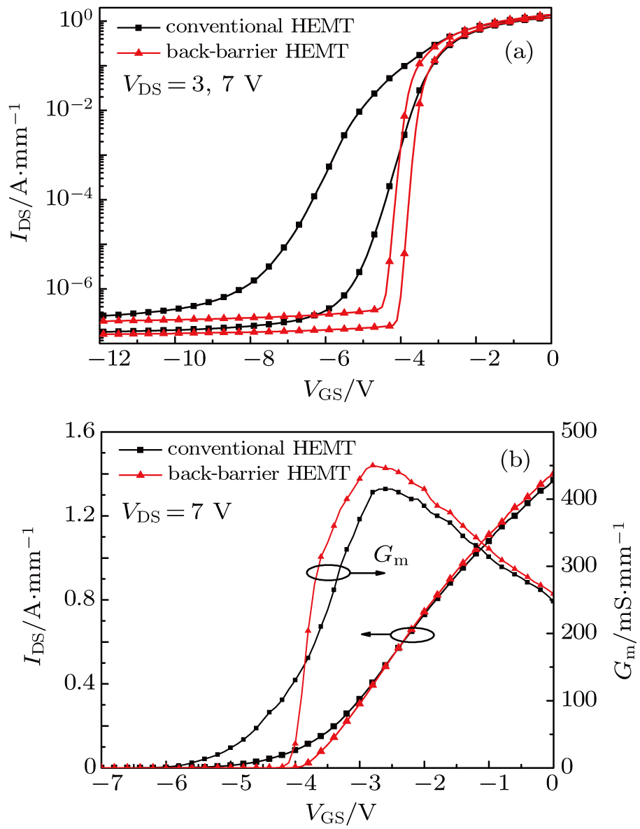
(color online) (a) IDS–VGS transfer characteristics plotted by the log-scale at VDS = 3 V and 7 V for InAlN/GaN HEMTs with and without back-barrier, respectively. (b) Gm–VGS and IDS–VGS transfer characteristics of the two devices at VDS = 7 V.
