† Corresponding author. E-mail:
Project supported by the National High-Technology Research and Development Program of China (Grant No. 2015AA034801), the Foundation of the State Key Laboratory of Mechanical Transmission of Chongqing University (Grant Nos. SKLMT-ZZKT-2017M15, SKLM-ZZKT-2015Z16, and SKLMT-KFKT-201419), the National Natural Science Foundation of China (Grant Nos. 11374359, 11304405, and 11544010), the Natural Science Foundation of Chongqing (Grant Nos. cstc2015jcyjA50035 and cstc2015jcyjA1660), the Fundamental Research Funds for the Central Universities, China (Grant Nos. 106112017CDJQJ328839, 106112014CDJZR14300050, 106112016CDJZR288805, and 106112015CDJXY300002), and the Sharing Fund of Large-scale Equipment of Chongqing University (Grant Nos. 201606150016, 201606150017, and 201606150056).
In order to decrease the Schottky barrier height and sheet resistance between graphene (Gr) and the p-GaN layers in GaN-based light-emitting diodes (LEDs), some transparent thin films with good conductivity and large work function are essential to insert into Gr and p-GaN layers. In this work, the ultra-thin films of four metals (silver (Ag), golden (Au), nickel (Ni), platinum (Pt)) are explored to introduce as a bridge layer into Gr and p-GaN, respectively. The effect of a different combination of Gr/metal transparent conductive layers (TCLs) on the electrical, optical, and thermal characteristics of LED was investigated by the finite element methods. It is found that both the TCLs transmittance and the surface temperature of the LED chip reduces with the increase of the metal thickness, and the transmittance decreases to about 80% with the metal thickness increasing to 2 nm. The surface temperature distribution, operation voltage, and optical output power of the LED chips with different metal/Gr combination were calculated and analyzed. Based on the electrical, optical, and thermal performance of LEDs, it is found that 1.5-nm Ag or Ni or Pt, but 1-nm Au combined with 3 layered (L) Gr is the optimal Gr/metal hybrid transparent and current spreading electrode for ultra-violet (UV) or near-UV LEDs.
Owing to their numerous advantages, such as high brightness, low energy consumption and long lifetime,[1,2] the GaN-LED have attracted extensive attention in the past few decades and been widely used in various fields including general lighting, traffic lights, automobile headlights, and backlight units for liquid crystal displays.[3,4] Usually the transparent conductive tin-doped indium oxide (ITO) is employed as the transparent electrode and current spreading layer for the contact on p-type GaN of LEDs. Although the device performance with ITO-based transparent p-type contacts has been improved, the exclusive uses of these oxides have faced serious problems due to the high cost, dwindling supply of indium, chemical instability in the presence of acids or alkali, and high processing temperature.[5,6] Furthermore, ITO shows extraordinary high absorption in the UV region, which makes it difficult to practically use as a transparent and current spreading electrode in UV LEDs. Hence, a transparent alternative electrode with the optical transmittance and electrical performances near to or better than those of the ITO layer is necessary.[7] Gr, which is formed of covalently bonded carbon atoms with a hexagonal lattice structure, is considered as an ideal ultra-thin two-dimensional candidate to replace conventional ITO electrodes because of its excellent optical and electrical properties. So a few investigations on the application of Gr as the transparent conducting electrodes in GaN-based LEDs have been reported recently.[8–10] However, due to the large difference of work function between the Gr (4.4 eV) and p-GaN layers (7.5 eV), a direct contact of Gr on the p-GaN layers will lead to a high sheet resistance and a large Schottky barrier height.[11–13] Therefore, forming a good Ohmic contact on the p-GaN layer is a key way to improve the performance of GaN-based LEDs with the Gr transparent electrodes layer.[14] To resolve these problems, ITO and NiOx as insertion layers between Gr and P-GaN have been investigated and some reasonable results have been achieved.[3,14] But there are still some problems to be solved, such as high work temperature of LED and unmatched conductivity between the electrode and p-GaN layers.[1,15] The metals (Ag, Au, Ni, Pt) possess good conductivity, high thermal conductivity, and large work function (Au/5.2 eV, Pt/5.7 eV, Ni/5.2 eV, Ag/4.4 eV, respectively) which are nearer to that of the p-GaN layer (7.5 eV). The insertion of an ultrathin metal material between the Gr layer and the p-GaN layer is expected to reduce the Schottky barrier, the contact resistance and the surface temperature if the metal is thin enough to make no significant optical loss.[12,16] Some work has been reported. For example, Ag nanowire,[7] Ni thin film,[12] Au nanocluster[17] were explored to insert between p-GaN and Gr to enhance the light output power in the UV LEDs, and Au-doped Gr was attempted by Seo et al.[13] and Kim et al.[16] These works indicate that the hybrid metal/Gr structure can be used as a transparent and current spreading electrode in UV or near-UV LEDs to improve the external quantum efficiency (EQE) and reduce the current crowding effect (CCE).[18] However, the influence of the thickness of the metal and Gr layers on the performance of LED and the optimal combination of Gr and different metal are still unknown. In the present work, the three-dimensional finite element simulation method is applied to analyze the effect of four kinds of metal/Gr hybrid structure (Ag/Gr, Au/Gr, Ni/Gr, and Pt/Gr) as the transparent electrode on the electrical, optical and thermal properties of GaN LEDs, and finally the optimal combination of Gr and metals (Ag, Au, Ni, Pt) is suggested.
In this work, semiconductor module, RF module, and Joule heating module in COMSOL Multiphysics software were used.
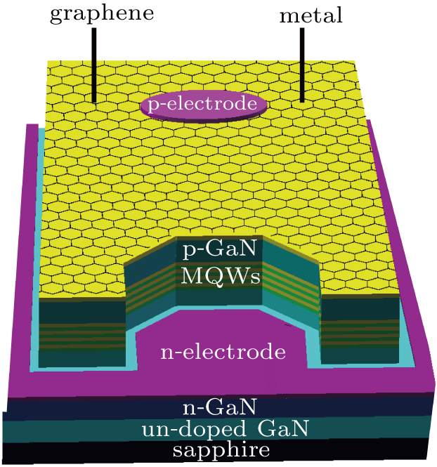
Numerical simulations for GaN LEDs have been proposed to overcome the technical challenges, including the thermal management and the current crowding phenomenon. We used the three-dimensional finite element method with the simulation software COMSOL to build the geometry model of the GaN-LED chip. Figure
 | Fig. 1. (color online) Schematic diagram of the GaN-LED chip with the transparent and current spreading electrode. |
| Table 1.
Physical parameters of various materials. Notes: sapphire and buffer layers are defined as heat transfer in a solid in the simulation procedure, thus their electrical conductivity is not needed. K: thermal conductivity, σ: electrical conductivity. . |
The steady-state method was used to simulate the Joule heat generation, the TCLs transmittance, and the operation voltage in GaN LEDs. The relationship between Joule heat Q,[19] current density J, and electrical field E is
 |
 |
 |
 |
 |
 |

 |
 |
 |
 |
 |
 |
Each layer of the GaN-LED chip is adopted as a homogeneous material.[30,31] The most concern for the approach is whether it is precise and accurate enough to predict the thermal and electrical performance of GaN-LED or not.[32] Based on the approximation between the simulation result and the experimental result of Seo et al.,[13] the original thermal and electrical parameters of different materials, which are derived from the literature, are adjusted considering the precision and accuracy of the Joule heat model. The final thermal and electrical parameters are listed in Table
The I–V characteristics, optical output powers and EQE of GaN-LEDs with Ag/Gr, Au/Gr, Ni/Gr, Pt/Gr, and Gr as TCLs were calculated through the semiconductor module. Figure
 | Fig. 2. (color online) (a) I–V characteristics and (b) optical output powers versus injection current and (c) EQE versus current curves of GaN-LEDs with Ag/Gr, Au/Gr, Ni/Gr, Pt/Gr and Gr as TCLs. |
Typically, the forward voltages at 20-mA current injection were 4.78 V, 3.91 V, 3.84 V, 3.92 V, and 6.03 V for GaN-LED with Ag/Gr, Au/Gr, Ni/Gr, Pt/Gr, and Gr, respectively. Compared with the experimental forward voltages of Au/Gr-LED (4.25 V) and Gr-LED (7.2 V) reported by Seo et al.,[17] the relative errors of the simulated voltage for Au/Gr-LED and Gr-LED are 8.0% and 16.25%, respectively. The errors may result from two factors: First, the boundary variables of metal and Gr in the simulation module were different from the experimental parameters;[17] second, an ideal Schottky contact was considered in the simulation model, but actually the contact between the electrode and GaN layer is not an ideal Schottky one. By the way, the Gr layer is usually regarded as smooth in the simulation work, but in fact it is maybe wrinkled on the p-GaN, while the metals (Ag, Au, Ni, and Pt) with a certain thickness are considered to be pyknotic and continuous in both simulation and practice, thus the relative error of Gr-LED operation voltage is larger than that of Au/Gr-LED.
Figure
From Fig.
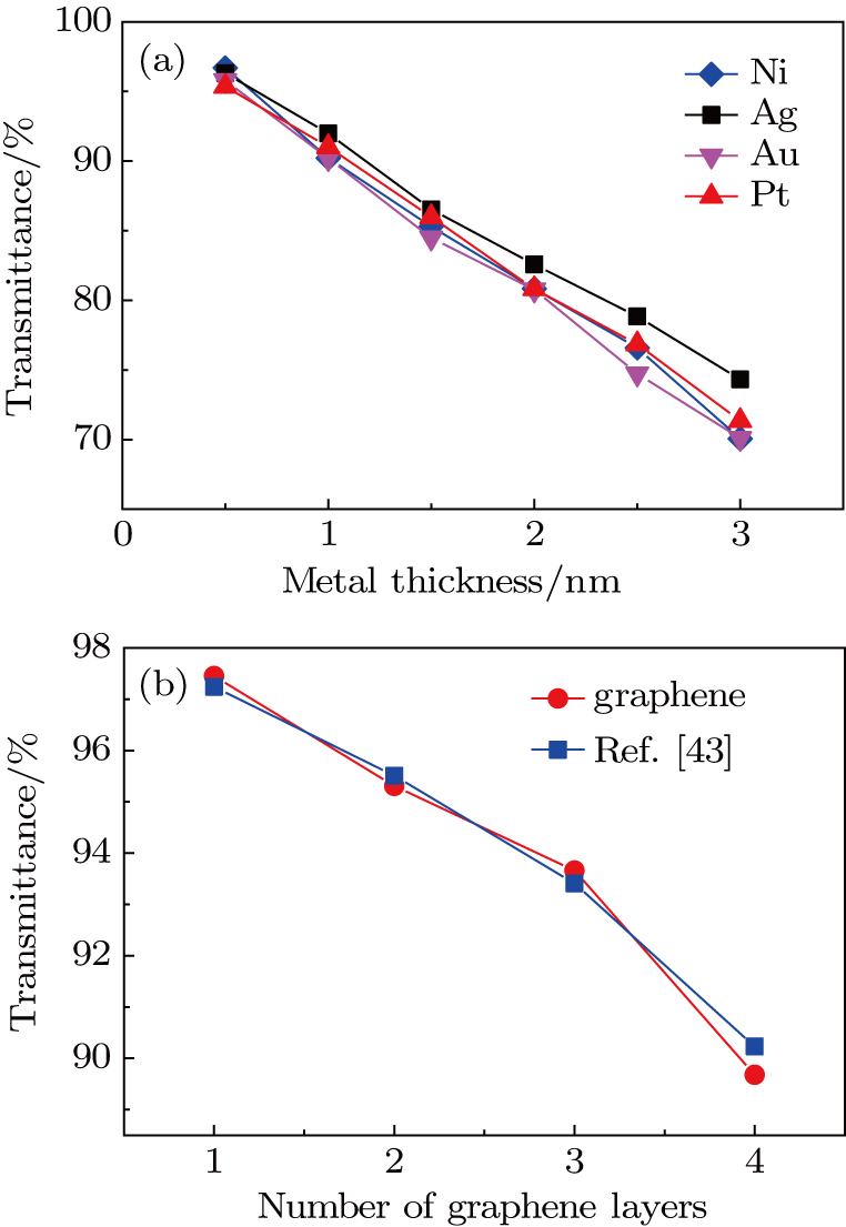
A high optical transmittance is indispensable when the top electrode film is used as the TCLs in LEDs. The light efficiency of LEDs strongly relies on the transmittance of TCLs. As displayed in Fig.
 | Fig. 3. (color online) (a) Optical transmittance characteristics of four metals at 550-nm wavelengths (b) optical transmittance characteristics of Gr layer at 550-nm wavelengths. |
Therefore, metal thickness is an important influential factor to cause optical loss. Figure
Optical transmittance of graphene with different layers and the metal (Ag, Au, Ni, Pt) with different thicknesses has been studied. The transmittance of visible light monotonously declines with the increase of the metal/Gr layers. However, the transmittances of metal (0.5 nm)/2L Gr and metal (2 nm)/3L Gr are still up to ~ 91% and ~ 80%, respectively, which are similar to those of the experiment results.[7,12,17] So metal/Gr was deemed to be potentially used in the LED chip as window electrodes.
The lower Tmax is important to get the better performance of the device.[44] The variation of the maximum temperature with 1L-Gr and the metal thickness was depicted in Fig.
 | Fig. 4. (color online) (a) Maximum temperature and (b) standard deviation of current density with 1 layer Gr and different thickness of metals. |
The effects of TCLs with the diverse combinations of Gr (1 ~ 4 layers) and metal (0.5 nm~ 3 nm) on the maximum temperature of the LED chip were calculated, and the results were shown in Fig.
 | Fig. 5. (color online) The Tmax distribution of LED with metal film and Gr layer at the injection current 20 mA. |
| Table 2.
The transmittance, Tmax and σj for metal/Gr optimization ratio. . |
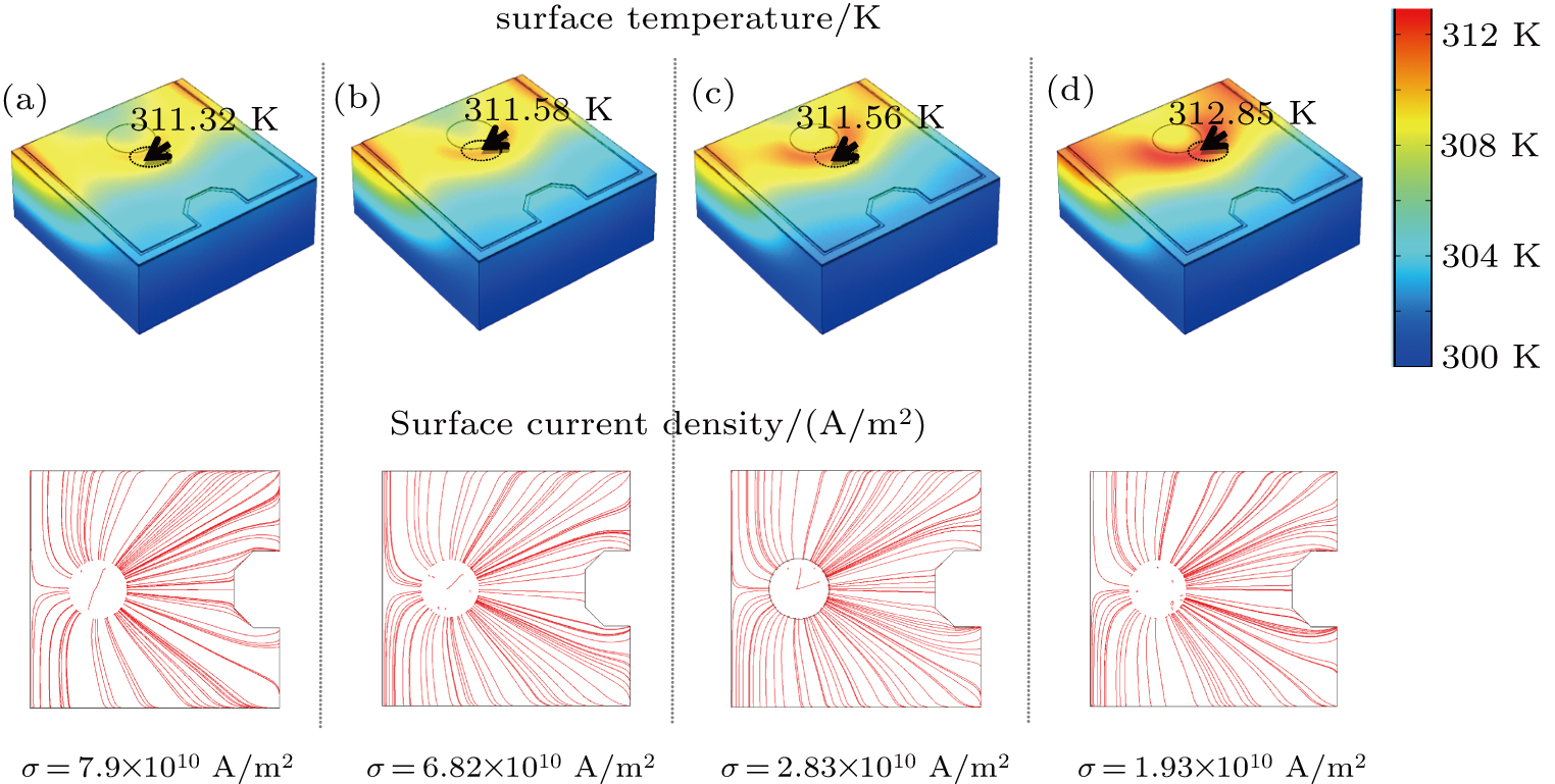
The distribution of the surfaces temperature and MQW current density of LEDs are shown in Fig.
In summary, the effect of different combinations of metal (Ag, Au, Ni, Pt) and Gr as the hybrid electrode and current spreading layers on the optical, thermal, and electrical performance of GaN-LEDs have been investigated. It shows that the metals inserted between Gr and p-GaN layer as a bridge layer can reduce the sheet resistance and contact resistance through a lower Schottky barrier, which improves the external quantum efficiency and optical output power and decreases the operation voltage. It is found that 1.5-nm Ag/3L Gr, 1-nm Au/3 L Gr, 1.5-nm Ni/3L Gr and 1.5-nm Pt/3L Gr as TCLs are the optimal combinations. Typically, when metal (Ag, Au, Ni, Pt)/3-layers Gr film hybrid TCLs are added, the temperature of LEDs could drop by about 12 K compared with that of only Gr as TCLs.
| [1] | |
| [2] | |
| [3] | |
| [4] | |
| [5] | |
| [6] | |
| [7] | |
| [8] | |
| [9] | |
| [10] | |
| [11] | |
| [12] | |
| [13] | |
| [14] | |
| [15] | |
| [16] | |
| [17] | |
| [18] | |
| [19] | |
| [20] | |
| [21] | |
| [22] | |
| [23] | |
| [24] | |
| [25] | |
| [26] | |
| [27] | |
| [28] | |
| [29] | |
| [30] | |
| [31] | |
| [32] | |
| [33] | |
| [34] | |
| [35] | |
| [36] | |
| [37] | |
| [38] | |
| [39] | |
| [40] | |
| [41] | |
| [42] | |
| [43] | |
| [44] | |
| [45] | |
| [46] |


