First principle study of edge topological defect-modulated electronic and magnetic properties in zigzag graphene nanoribbons
Huang Lu-Ting†, , Chen Zheng, Wang Yong-Xin, Lu Yan-Li
State Key Laboratory of Solidification Processing, School of Materials Science and Engineering, Northwestern Polytechnical University, Xi’an 710072, China


† Corresponding author. E-mail: hlt0922@mail.nwpu.edu.cn

Abstract

Zigzag graphene nanoribbon (ZGNR) is a promising candidate for next-generation spintronic devices. Development of the field requires potential systems with variable and adjustable electromagnetic properties. Here we show a detailed investigation of ZGNR decorated with edge topological defects (ED-ZGNR) synthesized in laboratory by Ruffieux in 2015 [Pascal Ruffieux, Shiyong Wang, Bo Yang, et al. 2015 Nature 531 489]. The pristine ED-ZGNR in the ground state is an antiferromagnetic semiconductor, and the acquired band structure is significantly changed compared with that of perfect ZGNR. After doping heteroatoms on the edge, the breaking of degeneration of band structure makes the doped ribbon a half-semi-metal, and nonzero magnetic moments are induced. Our results indicate the tunable electronic and magnetic properties of ZGNR by deriving unique edge state from topological defect, which opens a new route to practical nano devices based on ZGNR.

1. Introduction

Since graphene nanoribbons (GNRs) opened the band gap of two-dimensional (2D) graphene in the presence of edge states, they have soon aroused enormous interest of theorists and experimentalists in the relevant research field. Compared with armchair graphene nanoribbon (AGNR), zigzag graphene nanoribbon (ZGNR) is more concentrated due to its spin polarized edge states with ferromagnetic (FM) order at the same edge but antiferromagnetic (AFM) order between the opposite edges. Such a fascinating phenomenon in magnetism makes the ZGNR particularly applied to future spintronic devices used in memory storage, magnetic sensors and high speed computing equipment.[1]

Experimentally, ZGNR with varying widths can be realized by cutting carbon nanotubes (CNTs) or graphene. However, during its preparation, ZGNR is usually susceptible to various types of defect, such as vacancies, edge, hydrogen chemisorptions and topological defects.[25] Such defects could often induce its electronic and magnetic properties to change significantly, which may open new routes to practical nano devices based on ZGNR. Among these defects, topological defect could be deliberately introduced for manipulating the electronic properties of ZGNR, specially, asymmetry distribution of topological defect and the strain-induced ZGNR with topological defect lying in the middle produce obvious magnetism.[6,7] Meanwhile, topological defects transformation from center to edge is accompanied by a semiconductor-to-half-metal transition;[810] More interestingly, introducing heteroatoms (mainly nitrogen and boron atoms) into topological defect[2] makes us manipulate the magnetism and metallicity of ZGNR simultaneously. Thus, topological defect, together with topological doping, enable us to modulate the electronic properties more elaborately.

Recently, a new type of ZGNR with edge topological defect (ED-ZGNR) has been synthesized in laboratory, and it is an intermediate product of ZGNR in on-surface synthesis process.[11] To the best of our knowledge, there is no research on ZGNR with topological defect of its edges, and we speculate such a fresh edge state under reconstruction could bring in new intriguing performance of its electric and magnetic properties. Thus, we concentrate on the ED-ZGNR system in this paper, doping it with nitrogen (N), boron(B) atoms at different positions around the edge, and compare their energy band structures and spin distribution patterns in particular. The acquired result provides a qualitative reference to the designation of inorganic magnetic materials, which widens the application scope in spintronics.

2. Calculation methods

The generalized gradient approximation (GGA)[12,13] with the Perdew–Burke–Ernzerhof (PBE)[14] functional and a 500-eV cutoff for the plane-wave basis set were employed for all the density functional theory (DFT) computations with the Vienna ab initio simulation package (VASP).[15,16] The projector-augmented plane wave (PAW)[17,18] was used to model the electron–ion interaction. The Brillouin zone was sampled by 1×1×11 k-point meshes according to the Monkhorst–Pack scheme,[19] and the convergence threshold was set to be 1.0×10⁻⁵ eV in energy and 0.01 eV/Å in force. The positions of all the atoms in the unit cell were fully relaxed during the geometry optimization. On the basis of the equilibrium structure, 60 k points were used to compute band structure. To ensure the interaction between the defective ZGNRs, the vacuum of 15 Å is added both to neighboring cells and along the width direction.

3. Results and discussion
3.1. Pristine ED-ZGNR system

The STM image of 6-ED-ZGNR (six carbon zigzag lines wide, Fig. 1(a)) confirms the original structure (Fig. 1(b)) used in our study.[11] After geometry optimization, 6-ED-ZGNR maintains the sp2 hybrid orbitals of pristine ZGNR. Thus, certain electronic properties of ZGNR should survive in 6-ED-ZGNR. What is more, in contrast to the simplex zigzag edges (which determine the electronic states near Fermi level) of ZGNR, 6-ED-ZGNR possesses more complicated edges: zigzag cusps, quasi-edge, and phenyl (as shown in Fig. 1(b)). Accordingly, we also infer that besides the certain similar electronic properties, diverse electronic properties can also emerge between 6-ED-ZGNR and ZGNR. So, besides the certain similar electronic properties, diverse electronic properties are supposed to play a dominant role between 6-ED-ZGNR and ZGNR. In order to verify our speculation mentioned above, we systemically study the electromagnetic property of 6-ED-ZGNR in the following sections.
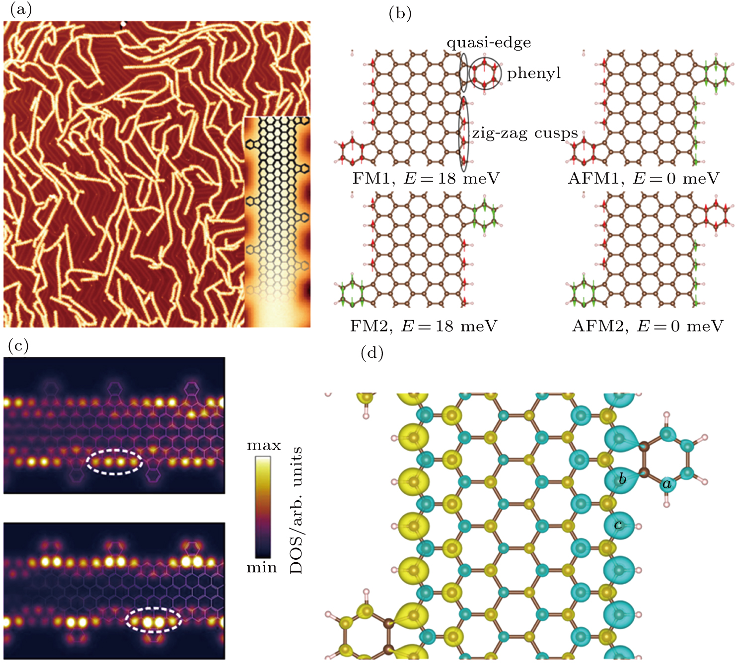
Fig. 1. (color online) (a) Overview STM image (V = −1.5 V, I = 150 pA) of 6-ED-ZGNRs fabricated on Au (111) surface with scale bar being 20 nm. Inset shows high-resolution STM image (V = 0.15 V, I = 2 pA), with scale bar being 1 nm;[11] (b) four different spin configurations on edges; (c) DFT-based density of states at E = −0.10 eV (corresponding to the highest occupied state) and E = 0.15 eV (corresponding to the lowest unoccupied level);[11] (d) spin-polarized charge density of 6-ED-ZGNR, with the spin-up and spin-down electron densities represented by the yellow and cyan colors, respectively.

The relaxed average bond length of edge C–C is 1.41 Å. As shown in Fig. 1(b), the edge of 6-ED-ZGNR is separated into three segments: zigzag cusps, quasi-edge, and phenyl. The zigzag cusps are identical to graphene nanoribbons, quasi-edge and phenyl constitute the edge-topological defect. This edge-topological defect disturbs the bipartite character of graphene lattice and breaks translational symmetry along the zigzag edge of graphene nanoribbons.[11] In addition, the electronic states near Fermi level stem mainly from the edge states (Fig. 1(c)). Thus, we speculate that there is difference in energy band between ED-ZGNR system and a perfect one, which determines its electronic performance.

In order to obtain precise band structure, we first identify the ground state of ED-ZGNR system. Since the perfect ZGNR is magnetically ordered, we only perform spin polarized calculations. The tested spin orientations between neighbor phenyl carbon atoms tend to be spin-consistent, so we only expect four spin configurations, which are shown in Fig. 1(b). Interestingly, FM2 and AFM2 configurations deviate from their initial arrangements to end in FM1 and AFM1 versions, respectively, and a lower energy of 18 meV of AFM2 reveals the AFM ground state of 6-ED-ZGNR. While the energy difference between AFM and FM in perfect 6-ZGNR is 26 meV,[20] our result shows weakened interedge magnetic interaction in the edge-defective ZGNR.[21] The corresponding spin density distribution (as displayed in Fig. 1(d)) shows that the magnetic moments are mainly localized around the edge, and resembles the spin density distribution of perfect ZGNR. Due to the charge of spin up and spin down compensating for each other completely, the total magnetic moment in a unit cell is zero.

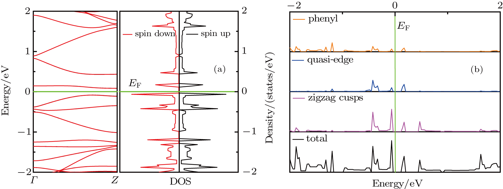
The band structure of 6-ED-ZGNR based on AFM ground state is plotted in Fig. 2(a). Just as we speculate, the energy bands is altered significantly by the edge topological modification.[22] In the vicinity of Fermi level, flat bands are achieved, which at the same time moves the locations of the valence band maximum (VBM) and the conduction band minimum (CBM), causing an indirect, narrower band gap of 0.17 eV than that of the perfect ZGNR.[11,21] The band gap is defined as –VBM, accordingly.[23] For a further understanding of electronic bands and individual contribution of atomic orbitals, the corresponding partial density of states (PDOS) profiles are investigated (Fig. 2(b)). As we have mentioned above, the edge state contributes to the density of state near the Fermi level, we discuss the effects of zigzag cusps, quasi-edge and phenyl atoms. On the one hand, since all the edge atoms are passivated by H atom, the function of σ dangling band is vanished and the energy bands for 6-ED-ZGNR only originate from the π character of bonds;[24] on the other hand, zigzag cusps make a major contribution to the bands near the Fermi level while the contribution of defect is quite trivial. The highest occupied molecular orbital (HOMO) is located on the energy level around −0.1 eV, which is most contributed by zigzag cusps, giving a very sharper peak on PDOS than others, while the lowest unoccupied molecular orbital (LUMO), corresponding to an energy level of 0.15 eV, in our study, stems from both zigzag cusps and quasi-edge atoms. They are equally dominant in density of state compared with the scenarios in Fig. 1(c), which emphasizes the highlights of quasi edge. Besides, both zigzag cusps and quasi-edge are atoms inherited from original zigzag edge of ZGNR, and their contributions to the flat bands are vital. After edge reconstruction, they still constitute predominantly to electronic state near the Fermi level while phenyl works weakly. So, whether could any differences be exerted on its electromagnetic property when heteroatoms are doped at phenyl, zigzag cusps and quasi-edge?

Fig. 2. (color online) (a) Band structure and the corresponding density of states (DOS) for 6-ED-ZGNR. The Fermi levels in the band structure and DOS are both set to be zero, and are indicated by the horizontal green line. (b) Partial densities of state (PDOSs) for 6-ED-ZGNR, where the Fermi level set to be zero is indicated by the vertical green line. The black, blue, magenta and orange lines denote TDOSs of zigzag cusps, quasi-edge and phenyl atoms, respectively.
3.2. Doped ED-ZGNR systems

For the exploitation of spin-polarized band structure and variable electromagnetic properties, doping pristine ED-ZGNR system with N, B atoms seems achievable. Just as indicated by our conclusion above, edge atoms play dominant role in forming energy bands near the Fermi level, and the existence of energy gap is also necessary for various applications in nano-electronics. When edge atoms are substituted, spin polarization may be controlled on the basis of reserving band gaps.

We consider three typical doping positions a, b, c (Fig. 1(d)), representing substitution on phenyl, quasi-edge, and zigzag cusps, respectively, and their basic parameters are listed in Table 1, including ground states, values of formation energy , net moments, band gap values as well as the average bond length between carbon and doping atoms . We first speculate the formation of the doped defective nanoribbons through the value of formation energy (), which is defined as , where and represent the total energies of the doped and pure ribbons, while and are the chemical potentials of the carbon (C) and dopant (N/B) atoms, respectively.[3] By analyzing the formation energies listed, we can find that N-doping is an exothermic process while B doping is an endothermic process, indicating the feasible synthesis of N-doped ribbons. The formation energies of the B doping are much less than those of transition metal-doped ribbons[25] which were recently synthesized in the laboratory doped at the edges. Therefore, the formation of B-doped defective ribbons is also realizable.[3] In addition, both N and B atoms s substituting for C atoms at zigzag cusps (N@c and B@c), are the most favorable configurations around others with the lowest formation energies of −1.4261 eV and 1.521 eV, respectively. After structure is optimized, the substitution leads to a slight local deformation. The average bond length between C and doping atoms decreases by N doping, while it increases by B. The reason lies in the difference between atomic radii. N has a smaller atomic radius than C, while B has a larger atomic radius than C. So, the value of decreases, whereas increases. The doped ribbons are fully relaxed into FM, AFM spin configurations, and lower energies reveal that they are all AFM ribbons. Besides, they all have magnetic moments close to one unit per unit cell. Since the band structure can reflect the magnetization of the system to some degree, the change of net moments should be a signature of band polarization.

Table 1.

Ground states, values of formation energy , magnetic moment, band gap values, and average bond lengths between carbon and doping atoms at different doping configurations of the doped ED-ZGNR systems.

.

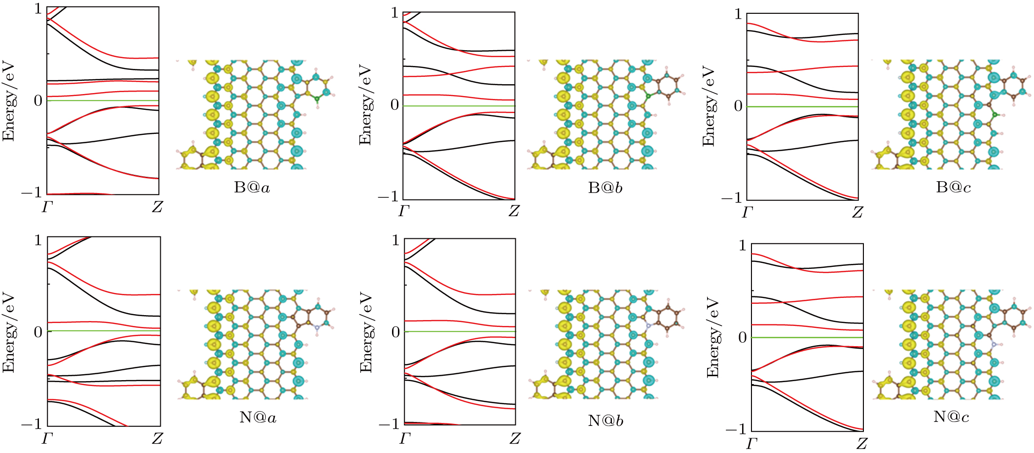
The corresponding band structures and spin distribution patterns based on their ground states are shown in Fig. 3. All doping ribbons possess spin-polarized band structures with the sub-bands close to the vicinity of Fermi level spliting into two spins (α, β). The breaking of degeneration together with reserved energy gap make the AFM ribbons half-semi-meatals,[26,27] in which the gap for α is significantly larger (above 0.28 eV) than that for β (below 0.16 eV). Only after tiny stimulation, spin-polarized current can be achieved if necessary. On the other hand, the spin charge densities reveal that spin charges on doped edge are greatly suppressed, especially in the defective area, while the undoped edge remains almost unchanged, resembles perfect ZGNR.[21] In consequence, the two spins are not balanced any more, giving rise to an existence of unpaired spin on the defect. The unpaired spin charge is responsible not only for induced magnetic moments but also for energy level splitting. According to previous studies, the existence of a heteroatom on the spin polarization pathway interrupts effective magnetic exchange,[2830] however, we find that kinds of dopants exhibit different ability to block magnetic interaction. In our study, the spin charges (both up spin and down spin) on defective atoms almost decrease to zero with N doping, which is in correspondence with two occupied bands (one α and one β) vanishing at the energy levels between 0.3 to 0.5 eV. But only part of spins are suppressed with B versions with most defective atoms possess spin density. Although significant differences emerge among their spin distributions, approximate magnetic moments are received after spin compensation, which is consistent with the data in Table 1.

Fig. 3. (color online) Band structures and corresponding spin distribution patterns of ED-ZGNR systems doped with N, B atoms substituting for C atoms at different positions a, b, c. The black and red lines denote the α and β states in the band structure, and the yellow and cyan colors refer to spin-up and spin–down electron densities, respectively. The Fermi level is marked by green line.

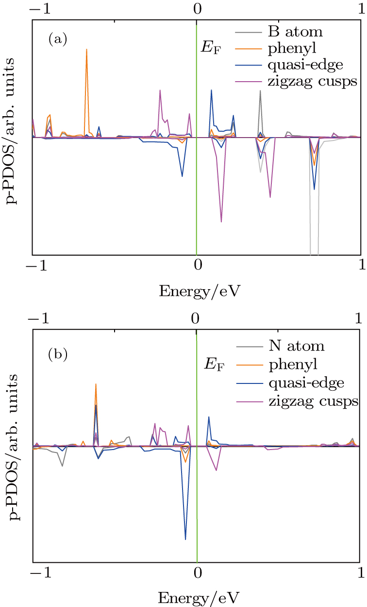
To further investigate the origins of the spin-resolved band structures and different blocking effects on heteroatoms (N/B), we exemplify the PDOSs of the most feasible ribbons B@c and N@c in Fig. 4. Firstly, with the contribution of quasi-edge around 0.1 eV, we can infer that the source of the split α spin at an energy level of −0.5 eV comes from a quasi-edge. Secondly, we find that N atom makes a key contribution to vanished energy bands because when B atoms substitutes for C atoms, obvious peaks in PDOS are shown to be around 0.3 eV, and it is mainly contributed by B atom. The calculated magnetic moment on each edge component (Table 2) also indicates that N atom suppresses more spin chargesat the same doping position, but lowers the magnetic moments compared with the substitution of B atoms.

Fig. 4. (color online) Plots of PDOS versus energy for (a) B@c ribbon, (b) N@c ribbon. The gray, blue, magenta and orange lines denote TDOS of B/N, zigzag cusps, quasi-edge, and phenyl atoms, respectively.
Table 2.

Magnetic moments of different edge components, including heteroatom (B/N), phenyl, quasi-edge, and zigzag cusps, respectively.

.
4. Conclusions

The electronic structure and magnetic properties of ZGNR decorated with edge topological defect are studied by using first-principle calculations. It is found that the pristine ED-ZGNR in the ground state is an AFM semiconductor. The edge topological defect breaks the integrity of graphene sub lattice, resulting in several flat bands in the vicinity of Fermi level, moving the positions of VBM and CBM, and causing a narrower band gap than that of the perfect ZGNR. The HOMO and LUMO are mainly provided by zigzag cusps and quasi-edge atoms in our study, which are atoms inherited from perfect ZGNR edges. After N, B atoms are doped at the different positions on the edge, both N and B atoms substituting for C atoms at zigzag cusps are the most favorable. The induced magnetic moments in doped ribbons are close to one unit per unit cell. At the same time, the pristine degenerate band structure becomes spin-split, and the breaking of degeneracy makes the doped ribbons half-semi-metals, which opens up the possibilities for spin polarized current. Both spin polarized band structure and induced magnetic moments stem from the asymmetric spin distribution caused by different blocking effects of heteroatom. Our study shows the interesting results of modulating variable and diverse properties of ZGNR, and the acquired half-semi-metals are quite promising candidates for future nanoelectronics, thereby expanding the application scope of graphene-based materials in spintronic field.

Reference
[1] Mandal B Sarkar S Pramanik A Sarkar P 2014 RSC Adv. 4 49946
[2] Baldoni M Sgamellotti A Mercuri F 2008 Chem. Phys. Lett. 464 202
[3] J. Bhattacharjee 2012 Chem. Phys. 137 094705
[4] Autes G Yazyev O V 2013 Phys. Rev. 87 3249
[5] Takazumi K Susumu O Kei K Kota D Kyoko N Yoshiyuki M 2006 Phys. Rev. 74 121412
[6] Lu P Zhang Z H Guo W L 2009 Phys. Lett. 373 3354
[7] Hu T Zhou J Dong J M Kawazoe Y 2012 Phys. Rev. 86 125420
[8] Lin X Q Ni J 2011 Phys. Rev. 84 075461
[9] Zhang W X He C Li T Gong S B 2015 RSC Adv. 5 33407
[10] Dai Q Q Zhu Y F Jiang Q 2013 Phys. Chem. 117 4791
[11] Ruffieux P Wang S Y Yang B Sánchez C Liu J Dienel T Talirz L Shinde P Pignedoli C A Passerone D Dumslaff T Feng X L Müllen K Fasel R 2015 Nature 531 489
[12] Perdew J P Chevary J A Vosko S H Jackson K A Pederson M R Singh D J Fiolhais C 1992 Phys. Rev. 46 6671
[13] Rasolt M Geldart D J W 1986 Phys. Rev. 34 1325
[14] Perdew J P Burke K Ernzerhof M 1996 Phys. Rev. Lett. 77 3865
[15] Kresse G Furthmüller 1996 Phys. Rev. 54 11169
[16] Kresse G Furthmuller 1996 Comput. Mater. Sci. 6 15
[17] Kresse G Joubert 1999 Phys. Rev. 59 1758
[18] Blöchl P E 1994 Phys. Rev. 50 17953
[19] Monkhorst H J Jack J D 1976 Phys Rev 13 5188
[20] Hou D Wei J Xie S 2010 Phys. Chem. 13 13202
[21] Cho D Ko K C Park H Lee J Y 2015 Phys. Chem. 119 10109
[22] Son Y W Cohen M L Louie S G 2006 Nature 444 347
[23] Li S Jiang Q Yang G W 2010 Appl. Phys. Lett. 96 213101
[24] Liu Y Chen Z Tong L J Zhang J Sun D Q 2016 Comput. Mater. Sci. 117 279
[25] Gorjizadeh N Farajian A A Esfarjani K Kawazoe Y 2008 Phys. Rev. 78 155427
[26] Pruneda J M 2010 Phys. Rev. 81 2149
[27] Rai H M Jaiswal N K Srivastava P Kurchania R 2013 Comput. Theor. Nanosci. 10 368
[28] Rajca A 2003 Chem. Eur. J. 8 4834
[29] Cho D Ko K C Lee J Y 2014 Phys. Chem. 118 5112
[30] Nam Y Cho D Jin Y L 2016 Phys. Chem. 120 11237