Spin-dependent transport characteristics of nanostructures based on armchair arsenene nanoribbons
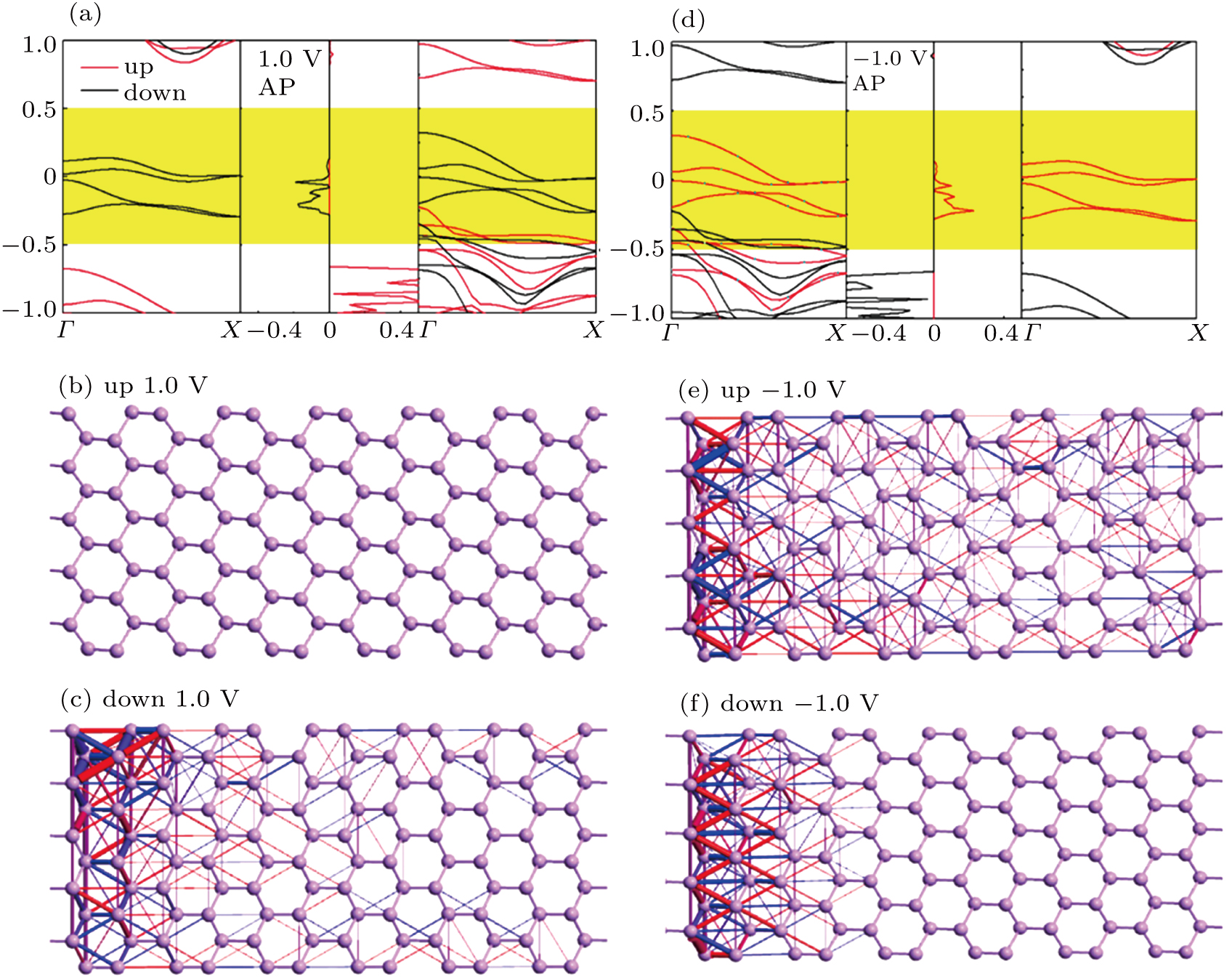
(color online) (a), (d) Left and right panels show the band structures of the left and right electrodes, and the middle panel displays the transmission spectrum of the scattering region for M3 device, correspond to bias of 1.0 V and −1.0 V, respectively. The zero of energy is set at Fermi level. (b), (c) Transmission paths (TPs) of spin-up and spin-down electrons under 1.0 V bias voltage. (e), (f) Transmission paths of spin-up and spin-down electrons under −1.0 V bias voltage, respectively.
