Optical response of tunable terahertz plasmon in a grating-gated graphene transistor
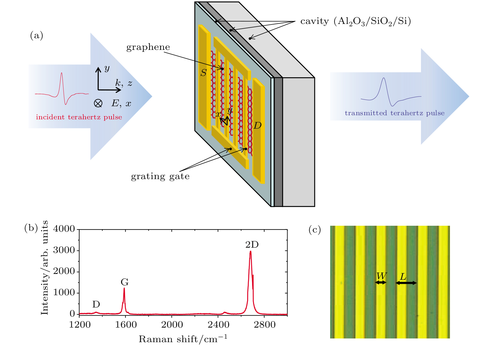
(color online) (a) Schematic structure of the device and the coordinate notation for transmission measurement. (b) Measured Raman spectrum of the transferred monolayer graphene on top of the Si/SiO2 substrate. (c) The optical photo of the grating gate.