Application of real space Kerker method in simulating gate-all-around nanowire transistors with realistic discrete dopants
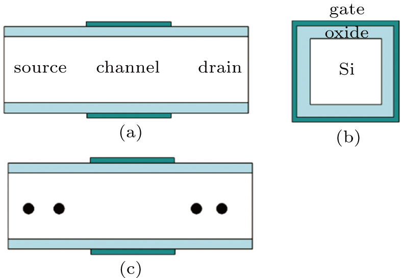
(color online) The structure of the gate all around silicon nanowire MOSFET considered in this work: (a) the cross section in the x–y plane, (b) the cross section in the y–z plane, and (c) two discrete dopants in the source region, and another two dopants in the drain region along the central line. In all the calculations, the silicon body thickness is 2 nm, and the oxide thickness is 1 nm.