Synthesis and magnetotransport properties of Bi2Se3 nanowires
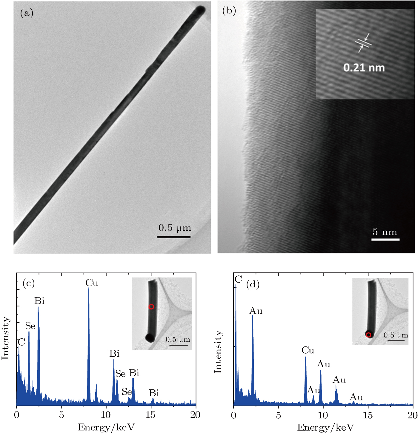
(color online) (a) TEM and (b) HRTEM images of a typical nanowire. The inset in panel (b) shows the lattice spacing of 0.21 nm. (c), (d) EDS spectra collected from the body and head of a single Bi2Se3 nanowire, respectively.