Microwave coherent manipulation of cold atoms in optically induced fictitious magnetic traps on an atom chip
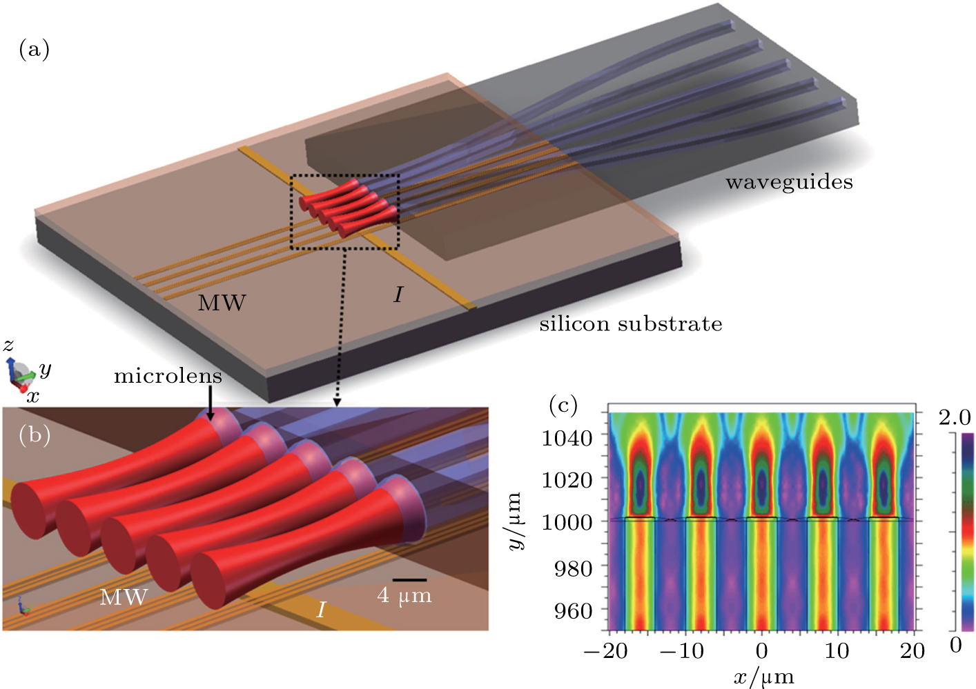
(color online) Schematic of the atom chip with integrated photonic waveguides. (a) The designed chip assembly consists of a gold wire chip and a photonic chip. The wire chip has a stationary current-carrying wire on the bottom layer for locating the OFMTs and four CPWs on the upper layer providing the microwave field for gate operation. (b) Schematic close-up of the experiment region. The photonic chip has 5 4-