Impact of energy straggle on proton-induced single event upset test in a 65-nm SRAM cell
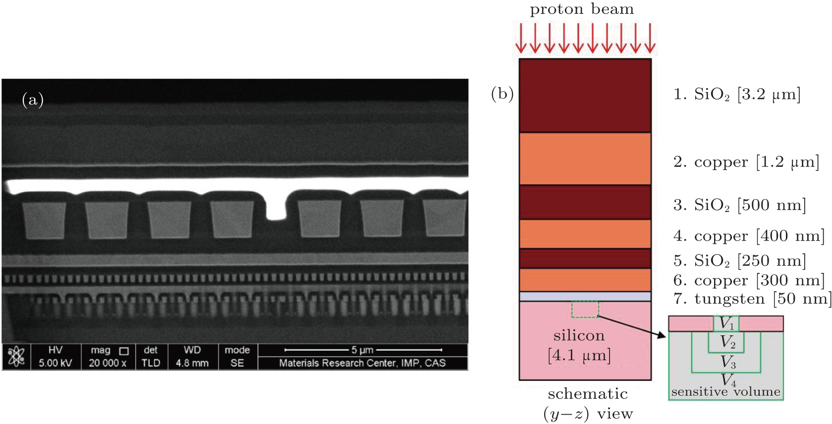
(color online) (a) The SEM view of the passivation and metallization layers. (b) Schematic chart of the multilayer structure and weighted SV model used in CRÈME-MC simulation of the device, with a cubic surface area of 10 μm × 10 μm. Not drawn exactly in accordance with the scale.